Features: • 1.8V Operation
• Designed to drive low impedance nets
• SSTL_18 style clock and data inputs
• Differential CLK input
• Control inputs compatible with LVCMOS levels
• Center input architecture for optimum PCB design
• Latch-up performance exceeds 100mA
• ESD >2000V per MIL-STD-883, Method 3015; >200V using machine model (C = 200pF, R = 0)
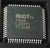
• Available in 150-pin CTBGA packageApplication• Along with CSPU877/A/D DDR2 PLL, provides complete solution for DDR2 DIMMs
• Optimized for DDR2-400/533 [PC2-3200/4300] Raw card LSpecifications
| Symbol |
Description |
Max. |
Unit |
| VDD |
Supply Voltage Range |
0.5 to 2.5 |
V |
| VI(2,3) |
Input Voltage Range |
0.5 to 2.5 |
V |
| VO(2,3) |
Output Voltage Range |
0.5 to VDD +0.5 |
V |
| IIK |
Input Clamp Current |
VI < 0 |
±50 |
mA |
| VI > VDD |
| IOK |
Output Clamp Current |
VO < 0 |
±50 |
mA |
| VO > VDD |
| IO |
Continuous Output Current,
VO = 0 to VDD |
±50 |
mA |
| VDD |
Continuous Current through each
VDD or GND |
±100 |
mA |
| TSTG |
Storage Temperature Range |
65 to +150 |
°C |
NOTES:
1. Stresses greater than those listed under ABSOLUTE MAXIMUM RATINGS may cause permanent damage to the device. This is a stress rating only and functional operation of the device at these or any other conditions above those indicated in the operational sections of this specification is not implied. Exposure to absolute maximum rating conditions for extended periods may affect reliability.
2. The input and output negative voltage ratings may be exceeded if the ratings of the I/P and O/P clamp current are observed.
3. This value is limited to 2.5V maximum.
DescriptionThe SSTU32D869 is a 14-bit 1:2 configurable registered buffer designed for 1.7V to 1.9V VDD operation. All clock and data inputs are compatible with the JEDEC standard for SSTL_18. The control inputs of IDT74SSTU32D869 are LVCMOS. All outputs are 1.8V CMOS drivers that have been optimized to drive the DDR2 DIMM load.
The SSTU32D869 operates from a differential clock (CLK and CLK). Data are registered at the crossing of CLK going high and CLK going low.
The SSTU32D869 includes a parity checking function. The SSTU32D869 accepts parity bits from the memory controller at its input pins PARIN[1:2], compares it with the data received on the D-inputs, and indicates whether a parity error has occured on its open-drain PTYERR[1:2] pins (active low).
When used as a single device, the C1 inputs are tied low. In this configuration of IDT74SSTU32D869, the partial-parity-out (PPO[1:2]) and PTYERR[1:2] signals are produced two clock cycles after the corresponding data output. When used in pairs, the C1 inputs of the first register are tied low and the C1 inputs of the second register are tied high. The PTYERR[1:2] outputs of the first SSTU32D869 is left floating and the valid error information is latched on the PTYERR[1:2] outputs of the second SSTU32D869 .
IDT74SSTU32D869 supports low-power standby operation. When the reset input (RESET) is low, the differential input receivers are disabled, and undriven (floating) data, clock, and reference voltage (VREF) inputs are allowed. In addition, when RESET IDT74SSTU32D869 is low all registers are reset, and all outputs are forced low. The LVCMOS RESET and Cx inputs must always be held at a valid logic high or low level.
To ensure defined outputs of IDT74SSTU32D869 from the register before a stable clock has been supplied, RESET must be held in the low state during power up.
In the DDR2 DIMM application, RESET is specified to be completely asynchronous with respect to CLK and CLK. Therefore, no timing relationship can be guaranteed between the two. When entering reset, the register will be cleared and the outputs of IDT74SSTU32D869 will be driven low quickly, relative to the time to disable the differential input receivers. However, when coming out of a reset, the register will become active quickly, relative to the time to enable the differential input receivers. As long as the data inputs are low, and the clock is stable during the time from the low-to-high transition of RESET until the input receivers are fully enabled, the design of the SSTU32D869 must ensure that the outputs will remain low, thus ensuring no glitches on the outputs.
IDT74SSTU32D869 monitors the DCS input and will gate the Qn outputs from changing states when DCS is high. If the DCS input is low, the Qn outputs will function normally. The RESET IDT74SSTU32D869 input has priority over the DCS control and will force the Qn outputs low and the PTYERR[1:2] outputs high. The EF[0:3] inputs control the driver strength and slew rate for both the A and B outputs independently.
IDT74SSTU32D869 also supports low-power active operation by monitoring both system chip select (DCS and CSR) inputs and will fate the Qn and PPO outputs from changing states when both DCS and CSR inputs are high. If either DCS and CSR input is low, the Qn and PPO outputs will function normally. Also, if the DCS and CSR are high, the device will gate the PTYERR[1:2] outputs from changing states. If the DCS and CSR are low, the PTYERR[1:2] IDT74SSTU32D869 will function normally. The RESET input has priority over the DCS and CSR control. When driven low, they will force the Qn and PPO outputs low and the PTYERR[1:2] outputs high. If theDCS control functionality is not desired, then the CSR input can be hard-wired to ground, in which case the setup-time requirement for the DCS would be the same as for the other D data inputs. To control the low-power mode of IDT74SSTU32D869 with DCS only, then the CSR input should be pulled up to VDD through a pullup resistor.

 IDT74SSTU32D869 Data Sheet