Features: • 28-bit 1:2 registered buffer with parity check functionality
• Supports SSTL_18 JEDEC specification on data inputs and outputs
• Supports LVCMOS switching levels on CSGateEN and RESET inputs
• Low voltage operation: VDD = 1.7V to 1.9V
• Available in 160-ball LFBGA packageApplication• DDR2 Memory Modules
• Provides complete DDR DIMM solution with ICS98ULPA877A or IDTCSPUA877A
• Ideal for DDR2 400, 533, 667, and 800Specifications
| Item |
Rating |
| Supply Voltage, VDD |
-0.5V to 2.5V |
| Input Voltage Range, VI1 |
-0.5V to VDD + 2.5V |
| Output Voltage Range, VO1,2 |
-0.5V to VDDQ + 0.5V |
| Input Clamp Current, IIK |
±50mA |
| Output Clamp Current, IOK |
±50mA |
| Continuous Output Clamp Current, IO |
±50mA |
| Continuous Current through each VDD or GND |
±100mA |
| Package Thermal Impedance (ja)3 |
0m/s Airflow |
44.3/W |
| 1m/s Airflow |
38.1/W |
| Storage Temperature |
-65 to +150 |
1 The input and output negative voltage ratings may be exceeded if the ratings of the I/P and
O/P clamp current are observed.
2 This current will flow only when the output is in the high state level VO > VDDQ.
3 The package thermal impedance is calculated in accordance with JESD 51.DescriptionThis 28-bit 1:2 registered buffer with parity is designed for 1.7V to 1.9V VDD operation.
All clock and data inputs are compatible with the JEDEC standard for SSTL_18. The control inputs are LVCMOS. All outputs are 1.8 V CMOS drivers that have been optimized to drive the DDR2 DIMM load. The IDT74SSTUBF32865A operates from a differential clock (CLK and CLK). Data are registered at the crossing of CLK going high, and CLK going low.
The device supports low-power standby operation. When the reset input (RESET) is low, the differential input receivers are disabled, and undriven (floating) data, clock and reference voltage (VREF) inputs are allowed. In addition, whenRESET is low all registers are reset, and all outputs except PTYERR are forced low. The LVCMOS RESET input must always be held at a valid logic high or low level.
To ensure defined outputs from the register before a stable clock has been supplied, RESET must be held in the low state during power up.
In the DDR2 RDIMM application, RESET is specified to be completely asynchronous with respect to CLK and CLK. Therefore, no timing relationship can be guaranteed between the two. When entering reset, the register will be cleared and the outputs will be driven low quickly, relative to the time to disable the differential input receivers. However, when coming out of reset, the register will become active quickly, relative to the time to enable the differential input receivers. As long as the data inputs are low, and the clock is stable during the time from the low-to-high transition of RESET until the input receivers are fully enabled, the design of the IDT74SSTUBF32865A must ensure that the outputs will remain low, thus ensuring no glitches on the output.
The device monitors both DCS0 and DCS1 inputs and will gate the Qn outputs from changing states when both DCS0 and DCS1 are high. If either DCS0 and DCS1 input is low, the Qn outputs will function normally. The RESET input has priority over the DCS0 and DCS1 control and will force the Qn outputs low and the PTYERR output high. If the DCS-control functionality is not desired, then the CSGateEnable input can be hardwired to ground, in which case, the setup-time requirement for DCS would be the same as for the other D data inputs.
The IDT74SSTUBF32865A includes a parity checking function. The IDT74SSTUBF32865A accepts a parity bit from the memory controller at its input pin PARIN, compares it with the data received on the D-inputs and indicates whether a parity error has occurred on its open-drain PTYERR pin (active LOW).

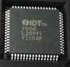
 IDT74SSTUBF32865A Data Sheet