Series: -
Type: -
On-State Resistance: -
Current - Output / Channel: -
Current - Peak Output: -
Mounting Type: Through Hole
Packaging: Tube
Input Type: Inverting
Number of Configurations: 1
High Side Voltage - Max (Bootstrap): 600V
Number of Outputs: 3
Manufacturer: International Rectifier
Voltage - Supply: 10 V ~ 20 V
Current - Peak: 250mA
Delay Time: 750ns
Configuration: 3 Phase Bridge
Operating Temperature: -
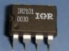
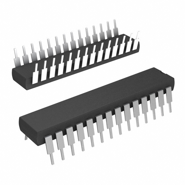
Package / Case: 28-DIP (0.600", 15.24mm)
Supplier Device Package: 28-DIP
Features: • Floating channel designed for bootstrap operation Fully operational to +600V or+1200V Tolerant to negative transient voltage dV/dt immune
• Gate drive supply range from 10V/12V to 20V DC and up to 25V for transient
• Undervoltage lockout for all channels
• Over-current shut down turns off all six drivers
• Independent 3 half-bridge drivers
• Matched propagation delay for all channels
• 2.5V logic compatible
• Outputs out of phase with inputs
• Also available LEAD-FREEPinout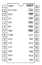 Specifications
| Symbol |
Definition |
Min. |
Max. |
Units |
| VB1,2,3 |
High Side Floating Supply Voltage |
(IR2133/IR2135) |
-0.3 |
625 |
V |
| (IR2233/IR2235) |
-0.3 |
1225 |
| VS1,2,3 |
High Side Floating Offset Voltage |
VB1,2,3 - 25 |
VB1,2,3 + 0.3 |
| VHO1,2,3 |
High Side Floating Output Voltage |
VS1,2,3 - 0.3
|
VB1,2,3 + 0.3 |
| VCC |
Low Side and Logic Fixed Supply Voltage |
-0.3 |
25 |
| VSS |
Logic Ground |
VCC - 25 |
VCC + 0.3 |
| VLO1,2,3 |
Low Side Output Voltage |
-0.3 |
VCC + 0.3 |
| VIN |
Logic input voltage (HIN, LIN, ITRIP, SD & FLT-CLR) |
VSS - 0.3 |
VCC + 0.3 or VSS +15
Which ever is lower |
| VIN,AMP |
Op amp input voltage (CA+ & CA-) |
VSS - 0.3 |
VCC + 0.3 |
| VOUT,AMP |
Op amp output voltage (CAO) |
VSS - 0.3 |
VCC + 0.3 |
| VFLT |
FAULT Output Voltage |
VSS - 0.3 |
VCC + 0.3 |
| dVS/dt |
Allowable Offset Supply Voltage Transient |
- |
50 |
V/ns |
| PD |
Package Power Dissipation @ TA +25 |
(28 Lead DIP) |
- |
1.5 |
W |
| (28 Lead SOIC) |
- |
1.6 |
| (44 Lead PLCC) |
- |
2.0 |
| RthJA |
Thermal Resistance, Junction to Ambient |
(28 Lead DIP) |
- |
83 |
/W |
| (28 Lead SOIC) |
- |
78 |
| (44 Lead PLCC) |
- |
63 |
| TJ |
Junction Temperature |
- |
150 |
|
| TS |
Storage Temperature |
-55 |
150 |
| TL |
Lead temperature (soldering, 10 seconds |
- |
300 |
DescriptionThe IR2133IR2135/IR2233IR2355 (J&S) are high voltage, high speed power MOSFET and IGBT driver with three independent high side and low side referenced output channels for 3-phase applications. Proprietary HVIC technology enables ruggedized monolithic construction. Logic inputs are compatible with CMOS or LSTTL outputs, down to 2.5V logic. An independent operational amplifier of IR2133IR2135/IR2233IR2355 provides an analog feedback of bridge current via an external current sense resistor. A current trip function which terminates all six outputs can also be derived from this resistor. A shutdown function is available to terminate all six outputs. An open drain FAULT signal is provided to indicate that an over-current or undervoltage shutdown has occurred. Fault conditions are cleared with the FLT-CLR lead. The output drivers feature a high pulse current buffer stage designed for minimum driver cross-conduction. Propagation delays are matched to simplify use in high frequency applications. The floating channels can be used to drive N-channel power MOSFETs or IGBTs in the high side configuration which operates up to 600 volts or 1200 volts.
Parameters: | Technical/Catalog Information | IR2133 |
| Vendor | International Rectifier |
| Category | Integrated Circuits (ICs) |
| Configuration | 3 Phase Bridge |
| Voltage - Supply | 10 V ~ 20 V |
| Current - Peak | 200mA |
| Delay Time | 750ns |
| Package / Case | 28-DIP (600 mil) |
| Packaging | Tube |
| Number of Outputs | 3 |
| Input Type | Inverting |
| Number of Configurations | 1 |
| Operating Temperature | - |
| High Side Voltage - Max (Bootstrap) | 600V |
| Lead Free Status | Contains Lead |
| RoHS Status | RoHS Non-Compliant |
| Other Names | IR2133
IR2133
|
 IR2133 Data Sheet