Features: • Internal self-timed write cycle
• Individual Byte Write Control and Global Write
• Clock controlled, registered address, data and control
• Pentium™ or linear burst sequence control using MODE input
• Three chip enable option for simple depth expansion and address pipelining
• Common data inputs and data outputs
• JEDEC 100-Pin TQFP and 119-pin PBGA package
• Single +3.3V, +10%, 5% power supply
• Power-down snooze mode
• 3.3V I/O For SPD
• 2.5V I/O For LPD
• Double cycle deselect
• Snooze MODE for reduced-power standby
• T version (three chip selects)
• D version (two chip selects)Pinout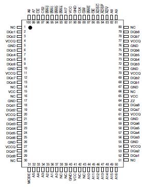 Specifications
| Symbol |
Parameter |
Value |
Unit |
| TBIAS |
Temperature Under Bias |
40 to +85 |
|
| TSTG |
Storage Temperature |
55 to +150 |
|
| PD |
Power Dissipation |
1.6 |
W |
| IOUT |
Output Current (per I/O) |
100 |
mA |
| VIN,VOUT |
Voltage Relative to GND for I/O Pins |
0.5 to VCCQ + 0.5 |
V |
| VIN |
Voltage Relative to GND for
for Address and Control Inputs |
0.5 to VCC + 0.5 |
V |
| VCC |
Voltage on Vcc Supply Relatiive to GND |
0.5 to 4.6 |
V |
Notes:
1. Stress greater than those listed under ABSOLUTE MAXIMUM RATINGS may cause permanent damage to the device. This is a stress rating only and functional operation of the device at these or any other conditions above those indicated in the operational sections of this specification is not implied. Exposure to absolute maximum rating conditions for extended periods may affect reliability.
2. This device contains circuity to protect the inputs against damage due to high static voltages or electric fields; however, precautions may be taken to avoid application of any voltage higher than maximum rated voltages to this high-impedance circuit.
3. This device contains circuitry that will ensure the output devices are in High-Z at power up.DescriptionThe ISSI IS61SPD25632, IS61SPD25636, S61SPD51218, IS61LPD25632, IS61LPD25636, and IS61LPD51218 are high-speed, low-power synchronous static RAMs designed to provide a burstable, high-performance, secondary cache for the Pentium™, 680X0™, and PowerPC™ microprocessors. The IS61SPD25632 and IS61LPD25632 are organized as 262,144 words by 32 bits and the IS61SPD25636 and IS61LPD25636 are organized as 262,144 words by 36 bits. The IS61LPD25632D and IS61LPS51218 are organized as 524,288 words by 18 bits. Fabricated with ISSI's advanced CMOS technology, the IS61LPD25632D integrates a 2-bit burst counter, high-speed SRAM core, and high-drive capability outputs into a single monolithic circuit. All synchronous inputs pass through registers controlled by a positive-edge-triggered single clock input.
Write cycles are internally self-timed and are initiated by the rising edge of the clock input. Write cycles can be from one to four bytes wide as controlled by the write control inputs.
Separate byte enables allow individual bytes to be written. Byte write operation is performed by using byte write enable (BWE).input combined with one or more individual byte write signals (BWx). In addition, Global Write (GW) is available for writing all bytes at one time, regardless of the byte write controls.
Bursts can be initiated with either ADSP (Address Status Processor) or ADSC (Address Status Cache Controller) input pins. Subsequent burst addresses can be generated internally and controlled by the ADV (burst address advance) input pin.
The mode pin is used to select the burst sequence order, Linear burst is achieved when this pin is tied LOW. Interleave burst is achieved when this pin is tied HIGH or left floating.

 IS61LPD25632D Data Sheet