KM718V987

Features: • Synchronous Operation.• On-Chip Address Counter.• Self-Timed Write Cycle.• On-Chip Address and Control Registers.• 3.3V+0.165V/-0.165V Power Supply.• I/O Supply Voltage 3.3V+0.165V/-0.165V for 3.3V I/O or 2.5V+0.4V/-0.125V for 2.5V I/O• 5V Tole...

product image

KM718V987 Picture
SeekIC No. : 004386187 Detail

KM718V987: Features: • Synchronous Operation.• On-Chip Address Counter.• Self-Timed Write Cycle.• On-Chip Address and Control Registers.• 3.3V+0.165V/-0.165V Power Supply.• ...

floor Price/Ceiling Price

Part Number:
KM718V987
Supply Ability:
5000

Price Break

  • Qty
  • 1~5000
  • Unit Price
  • Negotiable
  • Processing time
  • 15 Days
Total Cost: $ 0.00

SeekIC Buyer Protection PLUS - newly updated for 2013!

  • Escrow Protection.
  • Guaranteed refunds.
  • Secure payments.
  • Learn more >>

Month Sales

268 Transactions

Rating

evaluate  (4.8 stars)

Upload time: 2024/4/24

Payment Methods

All payment methods are secure and covered by SeekIC Buyer Protection PLUS.

Notice: When you place an order, your payment is made to SeekIC and not to your seller. SeekIC only pays the seller after confirming you have received your order. We will also never share your payment details with your seller.
Product Details

Description


Features:

• Synchronous Operation.
• On-Chip Address Counter.
• Self-Timed Write Cycle.
• On-Chip Address and Control Registers.
• 3.3V+0.165V/-0.165V Power Supply.
• I/O Supply Voltage 3.3V+0.165V/-0.165V for 3.3V I/O or 2.5V+0.4V/-0.125V for 2.5V I/O
• 5V Tolerant Inputs Except I/O Pins.
• Byte Writable Function.
• Global Write Enable Controls a full bus-width write.
• Power Down State via ZZ Signal.
• LBO Pin allows a choice of either a interleaved burst or a linear burst.
• Three Chip Enables for simple depth expansion with No Data Contention only for TQFP.
• Asynchronous Output Enable Control.
• ADSP, ADSC, ADV Burst Control Pins.
• TTL-Level Three-State Output.
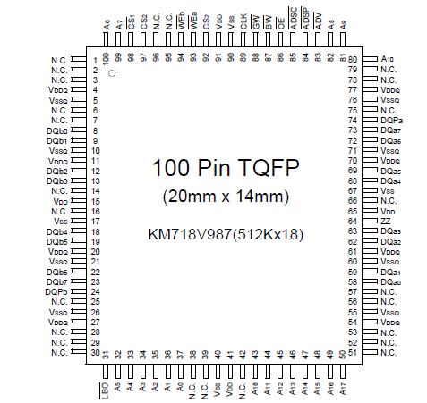
• 100-TQFP-1420A /119BGA(7x17 Ball Grid Array Package)


Pinout

  Connection Diagram


Specifications

PARAMETER
SYMBOL
RATING
UNIT
Voltage on VDD Supply Relative to VSS
VDD
-0.3 to 4.6
V
Voltage on VDDQ Supply Relative to VSS
VDDQ
VDD
V
Voltage on Input Pin Relative to VSS
VIN
-0.3 to 6.0
V
Voltage on I/O Pin Relative to VSS
VIO
-0.3 to VDDQ+0.5
V
Power Dissipation
PD
1.4
W
Storage Temperature
TSTG
-65 to 150
Operating Temperature
TOPR
0 to 70
Storage Temperature Range Under Bias
TBIAS
-10 to 85


Description

The KM718V987 and KM718V987 are 9,437,184-bit Synchronous Static Random Access Memory designed for high performance second level cache of Pentium and Power PC based System.

It is organized as 256K(512K) words of 36(18) bits and integrates address and control registers, a 2-bit burst addres counter and added some new functions for high performance  cache RAM applications; GW, BW, LBO, ZZ. Write cycles are internally self-timed and synchronous.

Full bus-width write is done by GW, and each byte write is performed by the combination of WEx and BW when GW is high. And with CS1 high, ADSP is blocked to control signals.

Burst cycle can be initiated with either the address status processor(ADSP) or address status cache controller(ADSC) inputs. Subsequent burst addresses are generated internally in the system¢s burst sequence and are controlled by the burst address advance(ADV) input.

LBO pin is DC operated and determines burst sequence(linear or interleaved).

ZZ pin controls Power Down State and reduces Stand-by current regardless of CLK.

The KM736V887 and KM718V987 are fabricated using SAMSUNG ¢s high performance CMOS technology and is available in a 100pin TQFP and 119BGA package. Multiple power and ground pins are utilized to minimize ground bounce.


Customers Who Bought This Item Also Bought

Margin,quality,low-cost products with low minimum orders. Secure your online payments with SeekIC Buyer Protection.
Prototyping Products
DE1
Batteries, Chargers, Holders
Semiconductor Modules
View more