SeekIC No. : 004391727
Detail
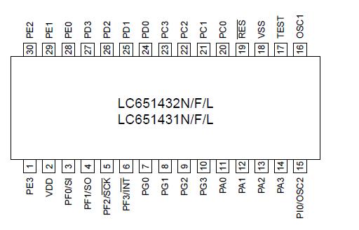
LC651432N: Features: • Fabricated in a CMOS process for low power operation (Standby mode can be controlled by CPU instructions.)• ROM/RAM LC651432N/F/L-ROM: 2 K *8 bits, RAM: 128 *4 bits LC651431N...
 LC651432N Data Sheet
floor Price/Ceiling Price
- Part Number:
- LC651432N
- Supply Ability:
- 5000
Price Break
- Qty
- 1~5000
- Unit Price
- Negotiable
- Processing time
- 15 Days
SeekIC Buyer Protection PLUS - newly updated for 2013!
- Escrow Protection.
- Guaranteed refunds.
- Secure payments.
- Learn more >>
Month Sales
268 Transactions
Payment Methods
All payment methods are secure and covered by SeekIC Buyer Protection PLUS.
Notice: When you place an order, your payment is made to SeekIC and not to your seller. SeekIC only pays the seller after confirming you have received your order. We will also never share your payment details with your seller.