DescriptionThe LC75824E is a kind of general-purpose LCD display driver. The device is intended for frequency display in microprocessor-controlled radio receivers and in other display applications. The device is able to directly drive up to 204 LCD segments. In addition, the device can control up ...
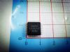
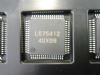
LC75824E: DescriptionThe LC75824E is a kind of general-purpose LCD display driver. The device is intended for frequency display in microprocessor-controlled radio receivers and in other display applications. ...
SeekIC Buyer Protection PLUS - newly updated for 2013!
268 Transactions
All payment methods are secure and covered by SeekIC Buyer Protection PLUS.
The LC75824E is a kind of general-purpose LCD display driver. The device is intended for frequency display in microprocessor-controlled radio receivers and in other display applications. The device is able to directly drive up to 204 LCD segments. In addition, the device can control up to 12 general-purpose output ports.
There are some features of LC75824E as follows: (1)support for 1/4-duty 1/2-bias or 1/4-duty 1/3-bias drive of up to 204 segments under serial data control; (2)serial data input supports CCB format communication with system controller; (3)serial data control of the power-saving mode based backup function and all the segments forced off function; (4)serial data control of switching between the segment output port and general-purpose output port functions; (5)serial data control of the normal mode current drain; (6)high generality since display data is displayed directly without decoder intervention; (7)the INH pin can force the display to the off state; (8)RC oscillator circuit.
The following is the absolute maximum ratings of LC75824E (Ta=25, VSS=0 V): (1)maximum supply voltage, VDD max: -0.3 to +7.0 V at pin VDD; (2)input voltage, VIN: -0.3 to +7.0 V at pins CE, CL, DI, INH and -0.3 to VDD+0.3 V at pins OSC, VDD1, VDD2; (3)output voltage, VOUT: -0.3 to VDD+0.3 V at pins OSC, S1 to S51, COM1 to COM4, P1 to P12; (4)output current, IOUT: 300A at pins S1 to S51, 3 mA at pins COM1 to COM4, 5 mA at pins P1 to P12; (5)allowable power dissipation, Pd max: 200 mW at Ta=65; (6)operating temperature, Topr: -40 to +85; (7)storage temperature, Tstg: -55 to +125.