LC876596B

Features: `Read-Only Memory (ROM): LC876596B 98304 * 8 bits LC876580B 81920 * 8 bits` Random Access Memory (RAM): LC876596B/80B 2048 * 9 bits` Minimum Bus Cycle Time: 100 ns (10 MHz) Note: The bus cycle time indicates ROM read time.` Minimum Instruction Cycle Time: 300 ns (10MHz)` Ports - Input/ou...

product image

LC876596B Picture
SeekIC No. : 004392490 Detail

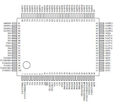
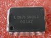
LC876596B: Features: `Read-Only Memory (ROM): LC876596B 98304 * 8 bits LC876580B 81920 * 8 bits` Random Access Memory (RAM): LC876596B/80B 2048 * 9 bits` Minimum Bus Cycle Time: 100 ns (10 MHz) Note: The bus c...

floor Price/Ceiling Price

Part Number:
LC876596B
Supply Ability:
5000

Price Break

  • Qty
  • 1~5000
  • Unit Price
  • Negotiable
  • Processing time
  • 15 Days
Total Cost: $ 0.00

SeekIC Buyer Protection PLUS - newly updated for 2013!

  • Escrow Protection.
  • Guaranteed refunds.
  • Secure payments.
  • Learn more >>

Month Sales

268 Transactions

Rating

evaluate  (4.8 stars)

Upload time: 2024/5/4

Payment Methods

All payment methods are secure and covered by SeekIC Buyer Protection PLUS.

Notice: When you place an order, your payment is made to SeekIC and not to your seller. SeekIC only pays the seller after confirming you have received your order. We will also never share your payment details with your seller.
Product Details

Description


Features:

`Read-Only Memory (ROM): LC876596B 98304 * 8 bits
                                             LC876580B 81920 * 8 bits
` Random Access Memory (RAM): LC876596B/80B 2048 * 9 bits
` Minimum Bus Cycle Time: 100 ns (10 MHz)
     Note: The bus cycle time indicates ROM read time.
` Minimum Instruction Cycle Time: 300 ns (10MHz)
` Ports
   - Input/output ports
    Data direction programmable for each bit individually :   20 (P1n, P70 to P73, P8n)
   - 15V withstand input/output ports
    Data direction programmable in nibble units :                 8 (P0n)
   (When N-channel open drain output is selected, data can be input in bit units.)
    Data direction programmable for each bit individually :   8 (P3n)
   - Input ports :                                                                   2 (XT1,XT2)
   - VFD output ports
     Large current outputs for digits :                                    9 (S0 / T0 to S8 / T8)
     Large current outputs for digits / segments :                 7 (S9 / T9 to S15 / T15)
    digit / segment outputs :                                                 8 (S16 to S23)
    segment outputs :                                                           28 (S24 to S51)
    Other functions
    Input/output ports :                                                        12(PFn, PG0 to 3)
    Input ports :                                                                    24 (PCn, PDn, PEn)
   - Oscillator pins :                                                               2 (CF1,CF2)
   - Reset pin :                                                                      1 (RES#)
   - Power supply :                                                                6 (VSS1 to 2, VDD1 to 4)
   - VFD power supply :                                                         1 (VP)
` VFD automatic display controller
   - Programmable segment/digit output pattern
     Output can be switched between digit/segment waveform output (pins 9 to 24 can be used for output of digit
waveforms.
    parallel-drive available for large current VFD.
   - 16-step dimmer function available
` Weak signal detection (MIC signals etc)
   - Counts pulses with width greater than a preset value
   - 2 bit counter
` Timers
   - Timer 0: 16 bit timer / counter with capture register
      Mode 0: 2 channel 8-bit timer with programmable 8 bit prescaler and 8 bit capture register
      Mode 1: 8 bit timer with 8 bit programmable prescaler and 8 bit capture register + 8 bit
      Counter with 8-bit capture register
      Mode 2: 16 bit timer with 8 bit programmable prescaler and 16 bit capture register
      Mode 3: 16 bit counter with 16 bit capture register
   - Timer 1: PWM / 16 bit timer toggle output
     Mode 0: 2 channel 8 bit timer (with toggle output)
     Mode 1: 2 channel 8 bit PWM
     Mode 2: 16 bit timer (with toggle output) Toggle output also possible using lower order 8 bits.
     Mode 3: 16 bit timer (with toggle output) Lower order 8 bits can be used as PWM output.
    - Base Timer
      1) The clock signal can be selected from any of the following : Sub-clock (32.768kHz crystal oscillator), system clock, and prescaler output from timer 0
     2) Interrupts can be selected to occur at one of five different times.
` Serial-interface
   - SIO 0: 8 bit synchronous serial Interface
     1) LSB first / MSB first function available
     2) Internal 8 bit baud-rate generator (maximum transmit clock period 4 / 3 Tcyc)
     3) Continuous automatic data communication (1-256 bits)
   - SIO 1: 8 bit asynchronous / synchronous serial interface
     Mode 0: Synchronous 8 bit serial IO (2-wire or 3-wire, transmit clock 2512 Tcyc)
     Mode 1: Asynchronous serial IO (half duplex, 8 data bits, 1 stop bit, baud rate 82048Tcyc)
     Mode 2: Bus mode 1 (start bit, 8 data bits, transmit clock 2512 Tcyc)
     Mode 3: Bus mode 2 (start detection, 8 data bits, stop detection)
` AD converter
   -8 bits * 12 channels
` Remote control receiver circuit (connected to P73 / INT3 / T0IN terminal)
   -Noise rejection function (noise rejection filter time constant can selected from 1 / 32 / 128 Tcyc)
` Watchdog timer
   - The watching timer period is set using an external RC.
   - Watchdog timer can produce interrupt, system reset
` Interrupts: 15-source, 10-vectored interrupts
    1) Three priority (low, high and highest) multiple interrupts are supported. During interrupt handling, an equal or
lower priority interrupt request is refused.
    2) If interrupt requests to two or more vector addresses occur at once, the higher priority interrupt takes precedence.
       In the case of equal priority levels, the vector with the lowest address takes precedence.
`Subroutine stack levels: 1024 levels max. Stack is located in RAM.
` Multiplication and division
   - 16 bit * 8 bit (executed in 5 cycles)
   - 24 bit * 16 bit (12 cycles)
   - 16 bit ÷ 8 bit (8 cycles)
   - 24 bit ÷ 16 bit (12 cycles)
` Oscillation circuits
   - On-chip RC oscillation circuit for system clock use.
   - On-chip CF oscillation circuit for system clock use. (Rf built in)
   - On-chip Crystal oscillation circuit low speed system clock use. (Rd, Rf external)
` Standby function
   - HALT mode
     HALT mode is used to reduce power consumption. Program execution is stopped. Peripheral circuits still operate but VFD display and some serial transfer operations stop.
    1) Oscillation circuits are not stopped automatically.
    2) Release occurs on system reset or by interrupt.
   -HOLD mode
     HOLD mode is used to reduce power consumption. Both program execution and peripheral circuits are  stopped.
    1) CF, RCand crystal oscillation circuits stop automatically.
    2) Release occurs on any of the following conditions.
         (1) input to the reset pin goes low
         (2) a specified level is input at least one of INT0, INT1, INT2
         (3) an interrupt condition arises at port 0
   -X'tal HOLD made
    X'tal HOLD mode is used to reduce power consumption. Program execution is stopped.
   All peripheral circuits except the base timer are stopped.
    1) CF and RC oscillation circuits stop automatically.
    2) Crystal oscillator is maintained in its state at HOLD mode inception.
    3) Release occurs on any an any of the following conditions
       (1) input to the reset pin goes low
       (2) a specified level is input to at least one of INT0, INT1, INT2
       (3) an interrupt condition arises at port 0
       (4) an interrupt condition arises at the base-timer
` Factory shipment
   -delivery form QIP100E
` Development tools
   - Evaluation chip: LC876096
   - Emulator: EVA62S + ECB876500 (Evaluation chip board) + SUB876500 + POD100QFP
   - Flash ROM version: LC87F65C8A


Pinout

  Connection Diagram


Specifications

Parameter Symbol Pins Conditions  
Ratings
unit
VDD[V]
min.
typ
max.
Maximum
supply voltage
VDDMAX VDD1,VDD2,
VDD3,VDD4
VDD1=VDD2=VDD3=VDD4  
-0.3
+7.0
V
Input voltage VI(1) XT1, XT2, CF1,RES    
-0.3
 
VDD+0.3
VI(2) VP     VDD-45
VDD+0.3
output voltage VO(1) S0/T0 to S15/T15    
VDD-45
VDD+0.3
Input/output
voltage
VIO(1) •Port 0: CMOS output
option
•Port 1
•Port 3: CMOS output
option
•Port 7
•Port 8
   
-0.3
 
VDD+0.3
VIO(2) •Port 0 open drain
•Port 3 open drain
   
-0.3
 
15
VIO(3) S16 to S51    
VDD-45
VDD+0.3
High
level
output
current
Peak
output
current
IOPH(1) Ports 1, 3
•CMOS output selected
•Current at each pin.
 
-10
mA
IOPH(2) Port71,72,73 Current at each pin  
-3
   
IOPH(3) S0/T0 to S15/T15 Current at each pin  
-30
   
IOPH(4) S16 to S51 Current at each pin  
-15
Total
output
current
IOAH(1) Port 0    
-30
IOAH(2) Port 1,3 The total of all pins.  
-30
IOAH(3) Port 7 The total of all pins.  
-5
IOAH(4) S0/T0 to S15/T15 The total of all pins  
-65
   
IOAH(5) S16 to S27 The total of all pins  
-60
IOAH(6) S28 to S39 The total of all pins  
-60
   
IOAH(7) S40 to S51 The total of all pins.  
-60
Low
level
output
current
Peak
output
curren
IOPL(1) Port 02, 03 For each pin.  
30
IOPL(2) •Port 00,01,04 to 07
•Port 1,3
For each pin  
20
IOPL(3) Ports 7, 8 For each pin  
5
Total
output
current
IOAL(1) Ports 0 For each pin  
60
IOAL(2) Ports 1,3 For each pin  
50
IOAL(3) Port 7,8
For each pin  
20
Maximum power
dissipation
Pdmax QIP100E
Ta=-30 to+70°C  
500
mW
Operating
temperature
range
Topr      
-30
70
Storage
temperature
range
Tstg      
-55
125


Description

The LC876596B and LC876580B are 8 bit single chip microcontrollers with the following on-chip functional blocks :

   - CPU: operable at a minimum bus cycle time of 100 ns
   - On-chip ROM Maximum Capacity : LC876596B 96K bytes
     LC876580B 80K bytes
   - On-chip RAM: 2048 bytes
   - VFD automatic display controller / driver
   - 16 bit timer / counter (can be divided into two 8 bit timers)
   - 16 bit timer / PWM (can be divided into two 8 bit timers)
   - timer for use as date / time clock
   - synchronous serial I/O port (with automatic block transmit / receive function)
   - asynchronous / synchronous serial I/O port
   - 12-channel × 8-bit AD converter
   - Weak signal detector
   - 15-source 10-vectored interrupt system

All of the above functions are fabricated on a single chip.


Customers Who Bought This Item Also Bought

Margin,quality,low-cost products with low minimum orders. Secure your online payments with SeekIC Buyer Protection.
Prototyping Products
DE1
Audio Products
Computers, Office - Components, Accessories
Cable Assemblies
View more