LC8900KQ

Features: • On-chip PLL circuit: enables the LSI operation to be synchronous to the transmitted EIAJ format input signals.• Four input pins and one output pin: The output pin enables the input data to be sent as they are.• Two data output function modes: 20-bit data LSB first mod...

product image

LC8900KQ Picture
SeekIC No. : 004392624 Detail

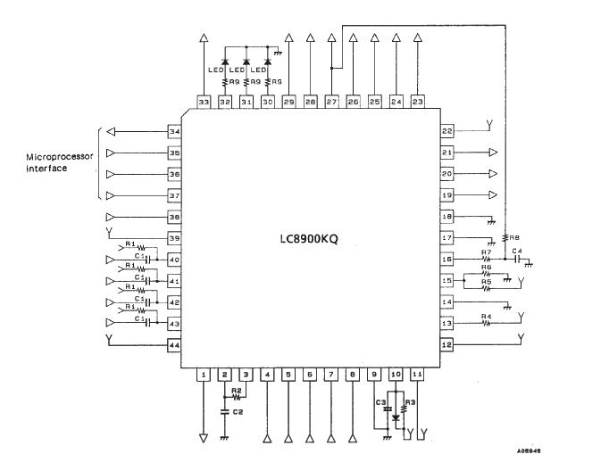
LC8900KQ: Features: • On-chip PLL circuit: enables the LSI operation to be synchronous to the transmitted EIAJ format input signals.• Four input pins and one output pin: The output pin enables the...

floor Price/Ceiling Price

Part Number:
LC8900KQ
Supply Ability:
5000

Price Break

  • Qty
  • 1~5000
  • Unit Price
  • Negotiable
  • Processing time
  • 15 Days
Total Cost: $ 0.00

SeekIC Buyer Protection PLUS - newly updated for 2013!

  • Escrow Protection.
  • Guaranteed refunds.
  • Secure payments.
  • Learn more >>

Month Sales

268 Transactions

Rating

evaluate  (4.8 stars)

Upload time: 2024/4/26

Payment Methods

All payment methods are secure and covered by SeekIC Buyer Protection PLUS.

Notice: When you place an order, your payment is made to SeekIC and not to your seller. SeekIC only pays the seller after confirming you have received your order. We will also never share your payment details with your seller.
Product Details

Description


Features:

• On-chip PLL circuit: enables the LSI operation to be synchronous to the transmitted EIAJ format input signals.
• Four input pins and one output pin: The output pin enables the input data to be sent as they are.
• Two data output function modes: 20-bit data LSB first mode and 16-bit data MSB first mode.
• Four output clocks: Bit clock, LRCK, 384Fs and 256Fs. All these clocks are synchronized to the data.
• Various signal outputs: copy inhibit, emphasis on:off control, user's bit, validity flag and sampling frequency.
• LPF time constant select mode: This function can be used in the PLL lock-up state.
• Error detect signal output: If an input data error is detected, this LSI circuit chip outputs the error signal. In this case, the previous data will be output by the chip.
• Lock-up signal output: This signal is output when the internal PLL (Phase Locked Loop) block of the LSI circuit chip is locked.
• The chip has the pin to receive a signal for stopping the PLL operation.
• Control and processing mode via microcontroller interface: input pin select, copy information and sampling frequency output.
• Each input pin has an internal amplifier circuit.
• Si gate, CMOS process technology and single 5V power supply applicational and functional concept.


Pinout

  Connection Diagram


Specifications

Parameter Symbol Conditions Ratings Unit
Maximum supply voltage VDD max Ta = 25 0.3 to +7.0 V
Input/output voltage VI, VO Ta = 25 0.3 to VDD +0.3 V
Ambient operating temperature Topr   30 to +75
Ambient storage temperature Tstg   55 to +125


Description

The LC8900KQ is a CMOS LSI circuit chip that can be used to enable the EIAJ CP-1201 formatted data transmission between digital audio equipment. It is used by the receiving end and operates synchronously with input signals. This chip demodulates input signals into normally-formatted signals.


Customers Who Bought This Item Also Bought

Margin,quality,low-cost products with low minimum orders. Secure your online payments with SeekIC Buyer Protection.
Cables, Wires
Power Supplies - Board Mount
Memory Cards, Modules
Test Equipment
Connectors, Interconnects
View more