Features: • 256K * 8 Bit Configuration
• 5 V Write/Erase (3.3 V VCC)
• Access Time
For 3.3 V Read: 150 ns
• Minimum 2.7 V Read Capability
180 ns Maximum Access Time (VCC = 2.7 V)
• 16 Independently Lockable Blocks (16K Blocks)
• 100,000 Erase Cycles per Block
• Automated Byte Write/Block Erase
Command User Interface
Status Register
• System Performance Enhancement
Erase Suspend for Read
Two-Byte Write
Full Chip Erase
• Data Protection
Hardware Erase/Write Lockout during Power Transitions
Software Erase/Write Lockout
• Independently Lockable for Write/Erase on Each Block (Lock Block and Protect Set/Reset)
• 80 A (MAX.) ICC in CMOS Standby
• State-of-the-Art 0.55 m ETOX™ Flash Technology
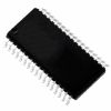
• Packages
32-Pin, 525-mil. SOP Package
32-Pin, 1.2 mm * 8 mm * 20 mm TSOP (Type I) Package
Pinout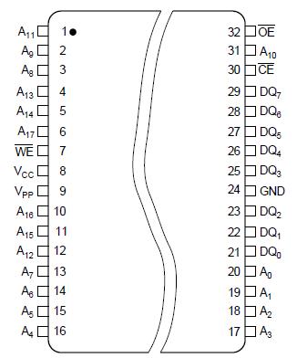 Specifications
Temperature Under Bias ....................... 0 to + 80
Storage Temperature ...................... -65 to + 125
*WARNING: Stressing the device beyond the "Absolute Maximum Ratings" may cause permanent damage. These are stress ratings only. Operation beyond the "Operating Conditions" is not recommended and extended exposure beyond the "Operating Conditions"may affect device reliability.
DescriptionThe LH28F020SU-L is a high performance 2M (2,097,152 bit) block erasable non-volatile random access memory organized as 256K × 8. The LH28F020SU-L includes sixteen 16K (16,384) blocks. A chip memory map is shown in Figure 4.
The implementation of a new architecture, with many enhanced features, will improve the device operating characteristics and results in greater product reliability and ease of use.
Among the significant enhancements of the LH28F020SU-L:
• 3 V Read, 5 V Write/Erase Operation (5 V VPP, 3 V VCC)
• Lower Power Capability (2.7 V VCC Read)
• Improved Write Performance
• Dedicated Block Write/Erase Protection
• Command-Controlled Memory Protection Set/Reset Capability
The LH28F020SUN-L12 will be available in a 32-pin, 525 mil. SOP package. This form factor and pinout allow for very high board layout densities.

 LH28F020SU-L Data Sheet