Features: · Fast Access Times: 20/25/35/50 ns
· Fast-Fall-Through Time Architecture Based on CMOS Dual-Port SRAM Technology
· Input Port and Output Port Have Entirely Independent Timing
· Expandable in Width and Depth
· Full, Half-Full, and Empty Status Flags
· Data Retransmission Capability
· TTL-Compatible I/O
· Pin and Functionally Compatible with Am/IDT7205
· Control Signals Assertive-LOW for Noise Immunity
· Package: 28-Pin, 300-mil PDIP
Pinout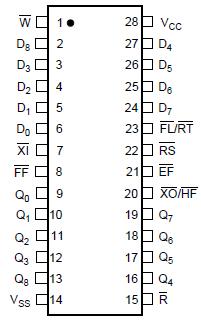 Specifications
| PARAMETER |
RATING |
| Supply Voltage to VSS Potential |
0.5 V to 7 V |
| Signal Pin Voltage to VSS Potential 2 |
0.5 V to VCC + 0.5 V (not to exceed 7 V) |
| DC Output Current 3 |
± 50 mA |
| Storage Temperature Range |
65 to 150 |
| Power Dissipation (Package Limit) |
1.0W |
| DC Voltage Applied to Outputs In High-Z State |
-0.5V |
NOTES:
1. Stresses greater than those listed under 'Absolute Maximum Ratings' may cause permanent damage to the device. This is a stress rating for transient conditions only. Functional operation of the device at these or any other conditions outside of those indicated in the 'Operating Range' of this specification is not implied. Exposure to absolute maximum rating conditions for extended periods may affect reliability.
2. Negative undershoots of 1.5 V in amplitude are permitted for up to 10 ns once per cycle.
3. Outputs should not be shorted for more than 30 seconds. No more than one output should be shorted at any time.
DescriptionThe LH540205 is a FIFO (First-In, First-Out) memory device, based on fully-static CMOS dual-port SRAM technology, capable of storing up to 8192 nine-bit words. It follows the industry-standard architecture and package pinouts for nine-bit asynchronous FIFOs. Each nine-bit LH540205 word may consist of a standard eight-bit byte, together with a parity bit or a block-marking/framing bit.
The input and output ports operate entirely independently of each other, unless the LH540205 becomes either totally full or else totally empty. Data flow at a port is initiated by asserting either of two asynchronous, assertive- LOW control inputs: Write (W) for data entry at the input port, or Read (R) for data retrieval at the output port.
Full, Half-Full, and Empty status flags monitor the extent to which the internal memory has been filled.
The system may make use of these status outputs to avoid the risk of data loss, which otherwise might occur either by attempting to write additional words into an already-full LH540205, or by attempting to read additional words from an already-empty LH540205. When an LH540205 is operating in a depth-cascaded configuration, the Half-Full Flag is not available. Data words are read out from the LH540205's output port in precisely the same order that they were written in at its input port; that is, according to a First-In, First Out (FIFO) queue discipline. Since the addressing sequence for a FIFO device's memory is internally predefined, no external addressing information is required for the operation of the LH540205 device.
Drop-in-replacement compatibility is maintained with both larger sizes and smaller sizes of industry-standard nine-bit asynchronous FIFOs. The only change is in the number of internally-stored data words implied by the states of the Full Flag and the Half-Full Flag.
The Retransmit (RT) control signal causes the internal FIFO-memory-array read-address pointer to be set back to zero, to point to the LH540205's first physical memory location, without affecting the internal FIFO-memoryarray write-address pointer. Thus, the Retransmit control signal provides a mechanism whereby a block of data, delimited by the zero physical address and the current write-address-pointer value, may be read out repeatedly an arbitrary number of times. The only restrictions are that neither the read-address pointer nor the write-address pointer may 'wrap around' during this entire process, i.e., advance past physical location zero after traversing the entire memory. The retransmit facility is not available when an LH540205 is operating in a depth-expanded configuration.

 LH540205 Data Sheet


