Features: ·2.7-V and 5-V Performance
·Low Supply Current:
LMV331 . . . 60 mA Typ
LMV393 . . . 100 mA Typ
LMV339 . . . 170 mA Typ
·Input Common-Mode Voltage Range Includes Ground
·Low Output Saturation Voltage . . . 200 mV Typ
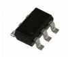
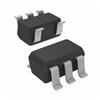
·Package Options Include Plastic Small-Outline (D), Small-Outline Transistor (SOT-23 DBV, SC-70 DCK), and Thin Shrink
Small-Outline (PW) PackagesPinout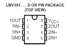
SpecificationsSupply voltage, VCC+ (see Note 1) . . . . . . . . . . . . . . . . . . . . . . . . . . . . . . . . . . . . . . .5.5 V
Differential input voltage, VID (see Note 2) . . . . . . . . . . . . . . . . . . . . . . . . . . . . . . .±5.5 V
Input voltage range, VI (either input). . . . . . . . . . . . . . . . . . . . . . . . . . . . . . . . . 0 to 5.5
Operating virtual junction temperature range . . . . . . . . . . . . . . . . . . . . . . . . . . 0 to 150
Package thermal impedance, qJA (see Notes 3 and 4): D (8-pin) package . . . . . . .97/W
D (14-pin) package . . . . . .86/W
DBV package . . . . . . . . . .347/W
DCK package . . . . . . . . . ..389/W
PW (8-pin) package . . . .. .149/W
PW (14-pin) package . . . ..113/W
Lead temperature 1,6 mm (1/16 inch) from case for 10 seconds: D or PW package . .260
Storage temperature range, Tstg . . . . . .65 to 150
† Stresses beyond those listed under "absolute maximum ratings" may cause permanent damage to the device. These are stress ratings only, and functional operation of the device at these or any other conditions beyond those indicated under "recommended operating conditions" is not implied. Exposure to absolute-maximum-rated conditions for extended periods may affect device reliability.
NOTES: 1. All voltage values (except differential voltages and VCC+ specified for the measurement of IOS) are with respect to the network GND.
2. Differential voltages are at IN+ with respect to IN.
3. Maximum power dissipation is a function of TJ(max), qJA, and TA. The maximum allowable power dissipation at any allowable ambient temperature is PD = (TJ(max) TA)/qJA. Selecting the maximum of 150°C can affect reliability.
4. The package thermal impedance is calculated in accordance with JESD 51.
DescriptionThe LMV393DUAL and LMV339 devices are low-voltage (2.7 V to 5.5 V) versions of the dual and quad comparators, LM393 and LM339, which operate from 5 V to 30 V. The LMV331 is the single-comparator version.
The LMV331, LMV339, and LMV393DUAL are the most cost-effective solutions for applications where low-voltage operation, low power, space saving, and price are the primary specifications in circuit design for portable consumer products. These devices offer specifications that meet or exceed the familiar LM339 and LM393 devices at a fraction of the supply current.
The LMV331 is available in the ultra-small DCK package, which is approximately one-half the size of the five-pin DBV package. The DCK package saves space on printed circuit boards and enables the design of small portable electronic devices. It also allows the designer to place the device closer to the signal source to reduce noise pickup and increase signal integrity.
The LMV331I, LMV393DUAL, and LMV393I devices are characterized for operation from 40 to 85.

 LMV393DUAL Data Sheet