LX1882

Features: ` Wide Input Voltage: 1.8V to 4.4V` 3.3V and Adjustable (2.5V to 5.5V) Output Voltage Options` Inductor-less design using small ceramic capacitors` Low Shutdown Current of 1A` Internal Thermal Shutdown and Current Limiting` 550kHz Switching OperationApplication· Cellular Telephone VCO Su...

product image

LX1882 Picture
SeekIC No. : 004403455 Detail

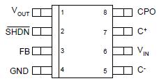
LX1882: Features: ` Wide Input Voltage: 1.8V to 4.4V` 3.3V and Adjustable (2.5V to 5.5V) Output Voltage Options` Inductor-less design using small ceramic capacitors` Low Shutdown Current of 1A` Internal The...

floor Price/Ceiling Price

Part Number:
LX1882
Supply Ability:
5000

Price Break

  • Qty
  • 1~5000
  • Unit Price
  • Negotiable
  • Processing time
  • 15 Days
Total Cost: $ 0.00

SeekIC Buyer Protection PLUS - newly updated for 2013!

  • Escrow Protection.
  • Guaranteed refunds.
  • Secure payments.
  • Learn more >>

Month Sales

268 Transactions

Rating

evaluate  (4.8 stars)

Upload time: 2024/4/18

Payment Methods

All payment methods are secure and covered by SeekIC Buyer Protection PLUS.

Notice: When you place an order, your payment is made to SeekIC and not to your seller. SeekIC only pays the seller after confirming you have received your order. We will also never share your payment details with your seller.
Product Details

Description


Features:

` Wide Input Voltage: 1.8V to 4.4V
` 3.3V and Adjustable (2.5V to 5.5V) Output Voltage Options
` Inductor-less design using small ceramic capacitors
` Low Shutdown Current of 1A
` Internal Thermal Shutdown and Current Limiting
` 550kHz Switching Operation


Application

· Cellular Telephone VCO Supplies
· Medical Instrumentation
· Data Acquisition
· Wireless PCMCIA Applications
· EMI Sensitive Boost Applications


Pinout

  Connection Diagram


Specifications

VIN to GND...............................................................-0.3V to 5V
VOUT Voltage...........................................................-0.3V to 6V
CPO to Ground................................................................... 10V
SHDN , FILT, FB Voltage to Ground............ -0.3V to (VIN + 0.3V)
VOUT Short Circuit Duration..................................... Indefinite
IOUT...................................................................................90mA
Operating Temperature Range
Commercial ........................................................... 0°C to 70°C
Storage Temperature ...................................... -65°C to 150°C
Lead Temperature (Soldering 10sec)................................300°C
Maximum Junction Temperature........................................125°C
Note: Exceeding these ratings could cause damage to the device. All voltages are with respect to Ground.
Currents are positive into, negative out of specified terminal.


Description

The LX1882 is a two-stage boost regulator featuring a charge pump doubler with an integrated low dropout linear regulator. This configuration allows for a low noise boosted output for powering noise sensitive applications.The first stage features an internal doubler charge pump converting an input supply of 1.8V to 4.4V, while the second stage is an LDO regulating the boosted voltage converting it to a low noise output.

The LX1882 is capable of supplying up to 50mA of output current with an operating current of less than 150A.Quiescent current is reduced to < 5A in shutdown mode.

The LX1882's internal regulator is stable with either Tantalum or Ceramic low-value cpacitors, typically 2.2F on the output,allowing designers flexibility in external component selection.Reliability and safety features include Thermal Shutdown Protection and Integrated Short-Circuit Protection.


Customers Who Bought This Item Also Bought

Margin,quality,low-cost products with low minimum orders. Secure your online payments with SeekIC Buyer Protection.
Tapes, Adhesives
803
Test Equipment
Resistors
Line Protection, Backups
Power Supplies - External/Internal (Off-Board)
View more