SeekIC No. : 004404514
Detail
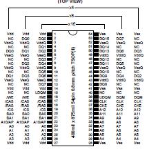
M2V56S40TP: Features: · Single 3.3v±0.3V power supply· Max. Clock frequency 100MHz(-7/-8), 133MHz (-6)· Fully Synchronous operation referenced to clock rising edge·Single Data Rate· 4 bank operation controlled ...
 M2V56S40TP Data Sheet
floor Price/Ceiling Price
- Part Number:
- M2V56S40TP
- Supply Ability:
- 5000
Price Break
- Qty
- 1~5000
- Unit Price
- Negotiable
- Processing time
- 15 Days
SeekIC Buyer Protection PLUS - newly updated for 2013!
- Escrow Protection.
- Guaranteed refunds.
- Secure payments.
- Learn more >>
Month Sales
268 Transactions
Payment Methods
All payment methods are secure and covered by SeekIC Buyer Protection PLUS.
Notice: When you place an order, your payment is made to SeekIC and not to your seller. SeekIC only pays the seller after confirming you have received your order. We will also never share your payment details with your seller.