Features: `MULTI-CHIP PACKAGE
1 die of 64 Mbit (4Mb x 16) Flash Memory
1 die of 16 Mbit (1Mb x 16) Pseudo SRAM
`SUPPLY VOLTAGE
VDDF = VDDP = 1.7V to 1.95V
`LOW POWER CONSUMPTION
`ELECTRONIC SIGNATURE
Manufacturer Code: 20h
Device Code (Top Flash Configuration), M36D0R6040T0: 8810h
Device Code (Bottom Flash Configuration), M36D0R6040B0: 8811h
`PACKAGE
Compliant with Lead-Free Soldering Processes
Lead-Free Versions
`PROGRAMMING TIME
8µs by Word typical for Fast FactoryProgram
Double/Quadruple Word Program option
Enhanced Factory Program options
`MEMORY BLOCKS
Multiple Bank Memory Array: 4 Mbit Banks
Parameter Blocks (Top location)
`ASYNCHRONOUS READ
Asynchronous Page Read mode
Random Access: 70ns
`DUAL OPERATIONS
Program Erase in one Bank while Read in others
No delay between Read and Write operations
`BLOCK LOCKING
All blocks locked at Power-up
Any combination of blocks can be locked
WPF for Block Lock-Down
`SECURITY
128-bit user programmable OTP cells
64-bit unique device number
`COMMON FLASH INTERFACE (CFI)
`100,000 PROGRAM/ERASE CYCLES per BLOCK
`ACCESS TIME: 70ns
`LOW STANDBY CURRENT: 110µA
`DEEP POWER DOWN CURRENT: 10µAPinout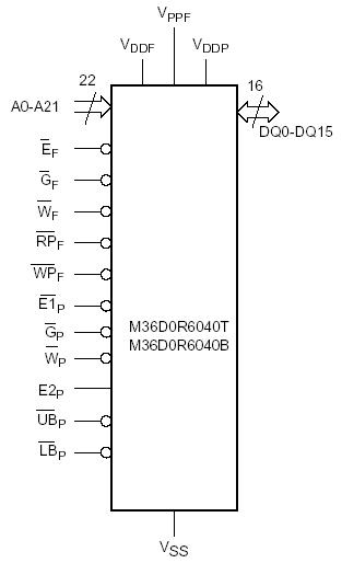 Specifications
| Symbol |
Parameter |
Value |
Unit |
| Min |
Max |
| TA |
Ambient Operating Temperature |
30 |
85 |
°C |
| TBIAS |
Temperature Under Bias |
-40 |
125 |
°C |
| TSTG |
Storage Temperature |
-65 |
155 |
°C |
| TLEAD |
Lead Temperature during Soldering |
|
(1) |
°C |
| VIO |
Input or Output Voltage |
-0.5 |
VDD(1)+0.6 |
V |
| VDDF |
Flash Memory Core Supply Voltage |
-0.2 |
2.45 |
V |
| VDDP |
PSRAM Supply Voltage |
-0.2 |
2.45 |
V |
| VPPF |
Flash Memory Program Voltage |
-0.2 |
14 |
V |
| IO |
Output Short Circuit Current |
|
100 |
mA |
| tVPPFH |
Time for VPPF at VPPFH |
|
100 |
hours |
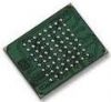
DescriptionThe M36D0R6040T0 and M36D0R6040B0 combine two memory devices in a Multi-Chip Package: a 64-Mbit, Multiple Bank Flash memory, the M58WR064FT/B, and a 16-Mbit Pseudo SRAM, the M69AR024B. Recommended operating conditions do not allow more than one memory to be active at the same time.
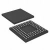
The memory M36D0R6040T0 and M36D0R6040B0 is offered in a Stacked TFBGA67 (12 x 8mm, 8x8 ball array, 0.8mm pitch) package. In addition to the standard version, the packages of M36D0R6040T0 and M36D0R6040B0 are also available in Lead-free version, in compliance with JEDEC Std J-STD-020B, the ST ECOPACK 7191395 Specification, and the RoHS (Restriction of Hazardous Substances) directive.
All packages of M36D0R6040T0 and M36D0R6040B0 are compliant with Lead-free soldering processes.
The memory of M36D0R6040T0 and M36D0R6040B0 is supplied with all the bits erased (set to '1').

 M36D0R6040B0 Data Sheet