Features: `MULTI-CHIP PACKAGE
1 die of 64 Mbit (4Mb x 16) Flash Memory
1 die of 16 Mbit (1Mb x 16) Pseudo SRAM
`SUPPLY VOLTAGE
VDDF = VDDP = 1.7V to 1.95V
`LOW POWER CONSUMPTION
`ELECTRONIC SIGNATURE
Manufacturer Code: 20h
Device Code (Top Flash Configuration), M36D0R6040T0: 8810h
Device Code (Bottom Flash Configuration), M36D0R6040B0: 8811h
`PACKAGE
Compliant with Lead-Free Soldering Processes
Lead-Free Versions
`PROGRAMMING TIME
8µs by Word typical for Fast FactoryProgram
Double/Quadruple Word Program option
Enhanced Factory Program options
`MEMORY BLOCKS
Multiple Bank Memory Array: 4 Mbit Banks
Parameter Blocks (Top location)
`ASYNCHRONOUS READ
Asynchronous Page Read mode
Random Access: 70ns
`DUAL OPERATIONS
Program Erase in one Bank while Read in others
No delay between Read and Write operations
`BLOCK LOCKING
All blocks locked at Power-up
Any combination of blocks can be locked
WPF for Block Lock-Down
`SECURITY
128-bit user programmable OTP cells
64-bit unique device number
`COMMON FLASH INTERFACE (CFI)
`100,000 PROGRAM/ERASE CYCLES per BLOCK
`ACCESS TIME: 70ns
`LOW STANDBY CURRENT: 110µA
`DEEP POWER DOWN CURRENT: 10µAPinout Specifications
| Symbol |
Parameter |
Value |
Unit |
| Min |
Max |
| TA |
Ambient Operating Temperature |
30 |
85 |
°C |
| TBIAS |
Temperature Under Bias |
-40 |
125 |
°C |
| TSTG |
Storage Temperature |
-65 |
155 |
°C |
| TLEAD |
Lead Temperature during Soldering |
|
(1) |
°C |
| VIO |
Input or Output Voltage |
-0.5 |
VDD(1)+0.6 |
V |
| VDDF |
Flash Memory Core Supply Voltage |
-0.2 |
2.45 |
V |
| VDDP |
PSRAM Supply Voltage |
-0.2 |
2.45 |
V |
| VPPF |
Flash Memory Program Voltage |
-0.2 |
14 |
V |
| IO |
Output Short Circuit Current |
|
100 |
mA |
| tVPPFH |
Time for VPPF at VPPFH |
|
100 |
hours |
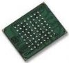
DescriptionThe M36D0R6040T0 and M36D0R6040B0 combine two memory devices in a Multi-Chip Package: a 64-Mbit, Multiple Bank Flash memory, the M58WR064FT/B, and a 16-Mbit Pseudo SRAM, the M69AR024B. Recommended operating conditions do not allow more than one memory to be active at the same time.
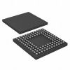
The memory of M36D0R6040T0 and M36D0R6040B0 is offered in a Stacked TFBGA67 (12 x 8mm, 8x8 ball array, 0.8mm pitch) package. In addition to the standard version, the packages are also available in Lead-free version, in compliance with JEDEC Std J-STD-020B, the ST ECOPACK 7191395 Specification, and the RoHS (Restriction of Hazardous Substances) directive.
All packages of M36D0R6040T0 and M36D0R6040B0 are compliant with Lead-free soldering processes.
The memory of M36D0R6040T0 and M36D0R6040B0 is supplied with all the bits erased (set to '1').

 M36D0R6040T0 Data Sheet