M50FLW040A

Features: `FLASH MEMORY Compatible with either the LPC interface or the FWH interface (Intel Spec rev1.1) used in PC BIOS applications 5 Signal Communication Interface supporting Read and Write Operations 5 Additional General Purpose Inputs for platform design flexibility Synchronized with 33MHz P...

product image

M50FLW040A Picture
SeekIC No. : 004405452 Detail

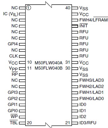
M50FLW040A: Features: `FLASH MEMORY Compatible with either the LPC interface or the FWH interface (Intel Spec rev1.1) used in PC BIOS applications 5 Signal Communication Interface supporting Read and Write Oper...

floor Price/Ceiling Price

Part Number:
M50FLW040A
Supply Ability:
5000

Price Break

  • Qty
  • 1~5000
  • Unit Price
  • Negotiable
  • Processing time
  • 15 Days
Total Cost: $ 0.00

SeekIC Buyer Protection PLUS - newly updated for 2013!

  • Escrow Protection.
  • Guaranteed refunds.
  • Secure payments.
  • Learn more >>

Month Sales

268 Transactions

Rating

evaluate  (4.8 stars)

Upload time: 2024/4/26

Payment Methods

All payment methods are secure and covered by SeekIC Buyer Protection PLUS.

Notice: When you place an order, your payment is made to SeekIC and not to your seller. SeekIC only pays the seller after confirming you have received your order. We will also never share your payment details with your seller.
Product Details

Description


Features:

`FLASH MEMORY
Compatible with either the LPC interface or the FWH interface (Intel Spec rev1.1) used in PC BIOS applications
5 Signal Communication Interface supporting Read and Write Operations
5 Additional General Purpose Inputs for platform design flexibility
Synchronized with 33MHz PCI clock
`8 BLOCKS OF 64 KBYTES
5 blocks of 64 KBytes each
3 blocks, subdivided into 16 uniform sectors of 4 KBytes each Two blocks at the top and one at the bottom (M50FLW040A) One block at the top and two at the bottom (M50FLW040B)
`ENHANCED SECURITY
Hardware Write Protect Pins for Block Protection
Register-based Read and Write Protection
`SUPPLY VOLTAGE
VCC = 3 to 3.6V for Program, Erase and Read Operations
VPP = 12V for Fast Program and Erase
`TWO INTERFACES
Auto Detection of Firmware Hub (FWH) or Low Pin Count (LPC) Memory Cycles for Embedded Operation with PC Chipsets
Address/Address Multiplexed (A/A Mux) Interface for programming equipment compatibility.
`PROGRAMMING TIME: 10s typical
`PROGRAM/ERASE CONTROLLER
Embedded Program and Erase algorithms
Status Register Bits
`PROGRAM/ERASE SUSPEND
Read other Blocks/Sectors during Program Suspend
Program other Blocks/Sectors during Erase Suspend
`ELECTRONIC SIGNATURE
Manufacturer Code: 20h
Device Code (M50FLW040A): 08h
Device Code (M50FLW040B): 28h


Pinout

  Connection Diagram


Specifications

Symbol
Parameter
Min.
Max.
Unit
TSTG
Storage Temperature
-65
150
°C
TLEAD
Lead Temperature during Soldering
See note 1
°C
VIO
Input or Output range 2
0.50
VCC + 0.6
V
VCC
Supply Voltage
0.50
4
V
VPP
Program Voltage
0.6
13
V
VESD
Electrostatic Discharge Voltage (Human Body model) 3
-2000
2000
V
Note: 1. Compliant with JEDEC Std J-STD-020B (for small body, Sn-Pb or Pb assembly), the ST ECOPACK® 7191395 specification, and the European directive on Restrictions on Hazardous Substances (RoHS) 2002/95/EU 2. Minimum voltage may undershoot to 2V for less than 20ns during transitions. Maximum voltage may overshoot to VCC + 2V for less than 20ns during transitions. 3. JEDEC Std JESD22-A114A (C1=100 pF, R1=1500 , R2=500 )


Description

The M50FLW040 is a 4 Mbit (512Kb x8) non-volatile memory that can be read, erased and reprogrammed.These operations can be performed using a single low voltage (3.0 to 3.6V) supply. For fast programming and fast erasing in production lines, an optional 12V power supply can be used to reduce the erasing and programming time.

The M50FLW040 memory is divided into 8 Uniform Blocks of 64 KBytes each, three of which are divided into 16 uniform sectors of 4 KBytes each (see APPENDIX A. for details). All blocks and sectors can be erased independently. So, it is possible to preserve valid data while old data is erased. Blocks can be protected individually to prevent accidental program or erase commands from modifying their contents.

Program and erase commands are written to the Command Interface of the memory. An on-chip Program/Erase Controller M50FLW040 simplifies the process of programming or erasing the memory by taking care of all of the special operations that are required to update the memory contents. The end of a program or erase operation can be detected and any error conditions identified. The command set to control the memory is consistent with the JEDEC standards.
Two different bus interfaces are supported by the memory:
` The primary interface, the FWH/LPC Interface, uses Intel's proprietary Firmware Hub (FWH) and Low Pin Count (LPC) protocol. This has been designed to remove the need for the ISA bus in current PC Chipsets. The M50FLW040 acts as the PC BIOS on the Low Pin Count bus for these PC Chipsets.
` The secondary interface, the Address/Address Multiplexed (or A/A Mux) Interface, is designed to be compatible with current Flash Programmers, for production line programming prior to fitting the device in a PC Motherboard.
The memory is supplied with all the bits erased (set to '1').


Customers Who Bought This Item Also Bought

Margin,quality,low-cost products with low minimum orders. Secure your online payments with SeekIC Buyer Protection.
Prototyping Products
DE1
Industrial Controls, Meters
RF and RFID
Inductors, Coils, Chokes
View more