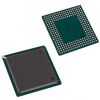
M59DR032EA

Features: ` SUPPLY VOLTAGEVDD = VDDQ = 1.65V to 2.2V for Program,Erase and ReadVPP = 12V for fast Program (optional)` ASYNCHRONOUS PAGE MODE READ Page Width: 4 Words Page Access: 35ns Random Access: 85ns, 100ns and 120ns` PROGRAMMING TIME 10µs by Word typical Double Word Program Option` MEMO...

product image

M59DR032EA Picture
SeekIC No. : 004406160 Detail

M59DR032EA: Features: ` SUPPLY VOLTAGEVDD = VDDQ = 1.65V to 2.2V for Program,Erase and ReadVPP = 12V for fast Program (optional)` ASYNCHRONOUS PAGE MODE READ Page Width: 4 Words Page Access: 35ns Random Access:...

floor Price/Ceiling Price

Part Number:
M59DR032EA
Supply Ability:
5000

Price Break

  • Qty
  • 1~5000
  • Unit Price
  • Negotiable
  • Processing time
  • 15 Days
Total Cost: $ 0.00

SeekIC Buyer Protection PLUS - newly updated for 2013!

  • Escrow Protection.
  • Guaranteed refunds.
  • Secure payments.
  • Learn more >>

Month Sales

268 Transactions

Rating

evaluate  (4.8 stars)

Upload time: 2024/5/9

Payment Methods

All payment methods are secure and covered by SeekIC Buyer Protection PLUS.

Notice: When you place an order, your payment is made to SeekIC and not to your seller. SeekIC only pays the seller after confirming you have received your order. We will also never share your payment details with your seller.
Product Details

Description


Features:

` SUPPLY VOLTAGE
VDD = VDDQ = 1.65V to 2.2V for Program,Erase and Read
VPP = 12V for fast Program (optional)
` ASYNCHRONOUS PAGE MODE READ
Page Width: 4 Words
Page Access: 35ns
Random Access: 85ns, 100ns and 120ns
` PROGRAMMING TIME
10µs by Word typical
Double Word Program Option
` MEMORY BLOCKS
Dual Bank Memory Array: 4 Mbit, 28 Mbit
Parameter Blocks (Top or Bottom location)
` DUAL BANK OPERATIONS
Read within one Bank while Program or Erase within the other
No delay between Read and Write operations
` BLOCK LOCKING
All blocks locked at Power up
Any combination of blocks can be locked
WP for Block Lock-Down
` COMMON FLASH INTERFACE (CFI)
64 bit Unique Device Identifier
64 bit User Programmable OTP Cells
` ERASE SUSPEND and RESUME MODES
` 100,000 PROGRAM/ERASE CYCLES per BLOCK
` 20 YEARS DATA RETENTION
Defectivity below 1ppm/year
` ELECTRONIC SIGNATURE
Manufacturer Code: 0020h
Top Device Code, M59DR032EA: 00A0h
Bottom Device Code, M59DR032EB: 00A1h


Specifications

Symbol Parameter Value Unit
TA Ambient Operating Temperature (1) 40 to 85 V
TBIAS Temperature Under Bias 40 to 125 V
TSTG Storage Temperature 55 to 155 V
VIO (2) Input or Output Voltage 0.5 to VDDQ+0.5
VDD, VDDQ Supply Voltage 0.5 to 2.7
VPP Program Voltage 0.5 to 13
Note: 1. Depends on range.
          2. Minimum Voltage may undershoot to 2V during transition and for less than 20ns.


Description

The M59DR032E is a 32 Mbit (2Mbit x16) non-vol- atile Flash memory that may be erased electrically at block level and programmed in-system on a Word-by-Word basis using a 1.65V to 2.2V VDD supply for the circuitry and a 1.65V to 2.2V VDDQ supply for the Input/Output pins. An optional 12V VPP power supply is provided to speed up custom- er programming.

The M59DR032E device features an asymmetrical block archi- tecture. M59DR032E has an array of 71 blocks and is divided into two banks, Banks A and B, pro-viding Dual Bank operations. While programming or erasing in Bank A, read operations are possible in Bank B or vice versa. Only one bank at a time is allowed to be in program or erase mode. The bank architecture is summarized in Table 2, and the Block Addresses are shown in Appendix A. The Parameter Blocks are located at the top of the memory address space for the M59DR032EA,and at the bottom for the M59DR032EB.

Each block M59DR032E can be erased separately. Erase can be suspended, in order to perform either read or program in any other block, and then resumed. Each block can be programmed and erased over 100,000 cycles.

M59DR032E Program and Erase commands are written to the Command Interface of the memory. An internal Program/Erase Controller takes care of the tim- ings necessary for program and erase operations.

The end of a program or erase operation can be detected and any error conditions identified in the Status Register. The command set required to control the memory is consistent with JEDEC stan- dards.

The M59DR032E features an instant, individual block locking scheme that allows any block to be locked or unlocked with no latency, enabling in- stant code and data protection. All blocks have two levels of protection. They can be individually locked and locked-down preventing any acciden- tal programming or erasure. All blocks are locked at Power Up and Reset.

The M59DR032E device includes a 128 bit Protection Register and a Security Block to increase the protection of a system's design. The Protection Register is di- vided into two 64 bit segments. The first segment contains a unique device number written by ST, while the second one is one-time-programmable by the user. The user programmable segment can be permanently protected. The Security Block, pa-rameter block 0, can be permanently protected by the user. Figure 4, shows the Security Block and Protection Register Memory Map.

The device M59DR032E is available in TFBGA48 (7 x 12mm and 7 x 7mm, 0.75mm pitch) packages and it is supplied with all the bits erased (set to '1').


Customers Who Bought This Item Also Bought

Margin,quality,low-cost products with low minimum orders. Secure your online payments with SeekIC Buyer Protection.
Test Equipment
Discrete Semiconductor Products
Line Protection, Backups
Soldering, Desoldering, Rework Products
Motors, Solenoids, Driver Boards/Modules
View more