Features: ·LOWPOWERDISSIPATION
ICC =4 mA (MAX.) AT TA =25°C
· COMPATIBLEWITH TTL OUTPUTS
VIH =2V(MIN)VIL = 0.8V(MAX) AT 5V
·OUTPUT DRIVECAPABILITY 90 LSTTL LOADS
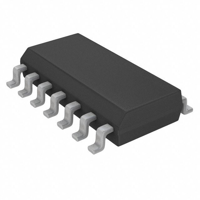
· HIGHCURRENT OPENDRAINOUTPUT UP TO80mAPinout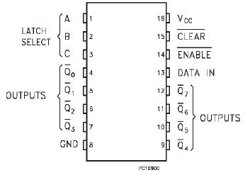 Specifications
| Symbol |
Parameter |
Value |
Unit |
| VCC |
Supply Voltage |
-0.5 to +7 |
V |
| VI |
DC Input Voltage |
-0.5 to VCC + 0.5 |
V |
| VO |
DC Output Voltage |
-0.5 to VCC + 0.5 |
V |
| IIK |
DC Input Diode Current |
± 20 |
mA |
| IOK |
DC Output Diode Current |
100 |
mA |
| IO |
DC Output Current |
- 800 |
mA |
| ICC |
DC VCC or Ground Current |
50 |
mA |
| PD |
Power Dissipation |
500(*) |
mW |
| Tstg |
Storage Temperature |
-65 to +150 |
°C |
| TL |
Lead Temperature (10 sec) |
300 |
°C |
AbsoluteMaximumRatingsarethose values beyond whichdamage to the device may occur. Functional operation under these condition isnot implied.
(*)500 mW: 65 derateto 300mWby 10mW/: 65 to85
DescriptionThe M74HCT7259 is a high speed CMOS 8 BIT ADDRESSABLE LATCH/DECODER fabricated in silicon gate C2MOS technology. It has the same high speed performance of LSTTL combined with true CMOS low power consumption.
The M74HCT7259 has single data input (D) 8 LATCH inverted OUTPUTS (Q0-Q7), 3 address inputs (A, B and C), common enable input (ENABLE) and a common CLEAR input. To operate this device as an addressable latch, data is held on the D input, and the address of the latch into which the data is to be entered is held on the A, B and C inputs.
When ENABLE is taken low the data flows through to the address output. The data of M74HCT7259 is stored on the positive-going edge of the ENABLE pulse. All unadressed latches will remain unaffected. With ENABLE in the high state the device is deselected and all latches remain in their previous state, unaffected by changes on the data or address inputs. To eliminate the possibility of entering erroneous data into the latches, the ENABLE should be held high (inactive) while the address lines are changing. If ENABLE is held high and CLEAR is taken low all eight latches are cleared to the HIGH (OFF) state. If ENABLE is low all latches except the addressed latch will be cleared. The address latch will instead be the complement of the D input,effectively implementing a 3 to 8 line decoder. Internal clamp diodes protect the open drain outputs against over voltages due to inductive loads.
All inputs of M74HCT7259 are equipped with protection circuits against static discharge and transient excess voltage.

 M74HCT7259 Data Sheet