Features: ` Integrated 16-Bit DAC and 16-Channel SHA with SRAM and Sequencer
` 16 Voltage Outputs
` 0.005% Output Linearity
` 200V Output Resolution
` Flexible Output Voltage Range
` Remote Ground Sensing
` Fast Sequential Loading: 1.3s per Register
` Burst and Immediate Mode Addressing
` No External Components Required for Setting Gain and Offset
` Integrated Output Clamp Diodes
` Three Output Impedance Options
MAX5621 (50), MAX5622 (500), and MAX5623 (1k)Application·MEMS Mirror Servo Control
·Industrial Process Control
·Automatic Test Equipment
·InstrumentationPinout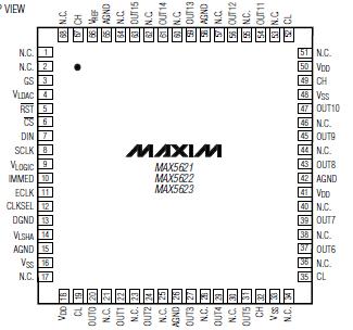 Specifications
VDD to AGND.......................................................-0.3V to +12.2V
VSS to AGND ........................................................-6.0V to +0.3V
VDD to VSS .........................................................................+15V
VLDAC, VLOGIC, VLSHA to AGND or DGND ..............-0.3V to +6V
REF to AGND............................................................-0.3V to +6V
GS to AGND................................................................VSS to VDD
CL and CH to AGND....................................................VSS to VDD
Logic Inputs to DGND .............................................-0.3V to +6V
DGND to AGND.........................................................-0.3V to +2V
Maximum Current into OUT_ ...........................................±10mA
Maximum Current into Logic Inputs ................................±20mA
Continuous Power Dissipation (TA = +70°C)
64-Pin TQFP (derate 13.3mW/°C above +70°C) ........1066mW
68-Pin Thin QFN (derate 28.6mW/°C above +70°C) ..2285mW
Operating Temperature Range .......................-40°C to +85°C
Maximum Junction Temperature ...................................+150°C
Storage Temperature Range .........................-65°C to +150°C
Lead Temperature (soldering, 10s) ..............................+300°C
Stresses beyond those listed under "Absolute Maximum Ratings" may cause permanent damage to the device. These are stress ratings only, and functional operation of the device at these or any other conditions beyond those indicated in the operational sections of the specifications is not implied. Exposure to absolute maximum rating conditions for extended periods may affect device reliability
DescriptionThe MAX5621/MAX5622/MAX5623 are 16-bit digital-toanalog converters (DACs) with 16 sample-and-hold (SHA) outputs for applications where a high number of programmable voltages are required. These devices include a clock oscillator and a sequencer that updates the DAC with codes from an internal SRAM. No external components are required to set offset and gain.
The MAX5621/MAX5622/MAX5623 feature a -4.5V to +9.2V output voltage range. Other features include a 200V/step resolution, with output linearity error, typically 0.005% of full-scale range (FSR). The 100kHz refresh rate updates each SHA every 320s, resulting in negligible output droop. Remote ground sensing allows the outputs to be referenced to the local ground of a separate device.
The MAX5623 is controlled through a 20MHz SPI™/QSPI™/MICROWIRE™-compatible 3-wire serial interface. Immediate update mode allows any channel's output to be updated within 20s. Burst mode allows multiple values to be loaded into memory in a single, high-speed data burst. All channels are updated within 330s after data has been loaded.
Each device features an output clamp and output resistors for filtering. The MAX5621 features a 50 output impedance and is capable of driving up to 250pF of output capacitance. The MAX5622 features a 500 output impedance and is capable of driving up to 10nF of output capacitance. The MAX5623 features a 1k output impedance and is capable of driving up to 10nF of output capacitance.
The MAX5621/MAX5622/MAX5623 are available in 64-pin TQFP (10mm x 10mm) and 68-pin thin QFN (10mm x 10mm) packages.

 MAX5623 Data Sheet