Features: High Accuracy ±2 (max) from +70 to +100(Remote)
11-Bit, 0.125°C Resolution
Dual Channel: Measures Remote and Local
Temperature
No Calibration Required
Programmable Under/Overtemperature Alarms
I2CTM-Compatible/SMBus Interface
+3V to +5.5V Supply Range
ApplicationDesktop Computers Workstations
Notebook Computers Test and Measurement
Servers Multichip Modules
Thin Clients
Pinout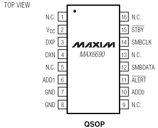 Specifications(All voltages are referenced to GND unless otherwise noted.)
VCC .........................................................................-0.3V to +6V
DXP, ADD_ .................................................-0.3V to (VCC + 0.3V)
DXN .....................................................................-0.3V to +0.8V
SMBCLK, SMBDATA, ALERT
, STBY.. ..........................-0.3V to +6V
SMBDATA, ALERT
Current .................................. -1mA to +50mA
DXN Current .....................................................................±1mA
ESD Protection (all pins, Human Body Model). .................2000V
Continuous Power Dissipation (TA = +70)
16-Pin QSOP (derate 8.30mW/ above +70)..............667mW
Operating Temperature Range ..........................-55 to +125
Junction Temperature......................................................+150
Storage Temperature Range ............................- 65 to +165
Lead Temperature (soldering, 10s) ............................... +300DescriptionThe MAX6690† is a precise digital thermometer thatreports the temperature of both a remote P-N junctionand its own die. The remote junction can be a diode-connectedtransistor-typically a low-cost, easily mounted2N3904 NPN type or 2N3906 PNP type-that replacesconventional thermistors or thermocouples. Remoteaccuracy is ±2 for multiple transistor manufacturers,with no calibration needed. The remote junction of MAX6690 can alsobe a common-collector PNP, such as a substrate PNP ofa microprocessor (µP).
The 2-wire serial interface of MAX6690 accepts standard SystemManagement Bus (SMBusTM), Write Byte, Read Byte,Send Byte, and Receive Byte commands to program thealarm thresholds and to read temperature data.Measurements can be done automatically andautonomously, with the conversion rate programmed bythe user, or programmed to operate in a single-shotmode. The adjustable conversion rate of MAX6690 allows the user tooptimize supply current and temperature update rate tomatch system needs. When the conversion rate is fasterthan 1Hz, the conversion results are available as a 7-bitplus-sign byte with a 1°C LSB. When the conversion rateis 1Hz or slower, the MAX6690 enters the extendedmode. In this mode, 3 additional bits of temperature dataare available in the extended resolution register, providing10-bit-plus-sign resolution with a 0.125 LSB.Single-shot conversions also have 0.125 per LSB resolutionwhen the conversion rate is 1Hz or slower.
A parasitic resistance cancellation (PRC) mode of MAX6690 can alsobe invoked for conversion rates of 1Hz or slower by settingbit 4 of the configuration register to 1. In PRC mode,the effect of series resistance on the leads of the externaldiode is canceled. The 11-bit conversion in PRC mode isperformed in <500ms and is disabled for conversionrates faster than 1Hz. The one-shot conversion is also 11bits in <500ms.
The MAX6690 default low-temperature measurementlimit is 0. This can be extended to -64 by setting bit5 of the configuration register to 1.
The MAX6690 is available in a small, 16-pin QSOP surface-mount package.

 MAX6690 Data Sheet