Features: ♦ Single Cell, 0.9V to 1.8V Single-Supply Operation
♦ Fixed Gain Eliminates External Feedback Network
MAX9721A: -2V/V
MAX9721B: -1.5V/V
MAX9721C: -1V/V
♦ Ground-Referenced Outputs Eliminate DC Bias
♦ No Degradation of Low-Frequency Response Due to Output Capacitors
♦ 20mW per Channel into 32Ω
♦ Low 0.006% THD+N
♦ High PSRR (80dB at 1kHz)
♦ Integrated Click-and-Pop Suppression
♦ Low Quiescent Current (2.2mA)
♦ Low-Power Shutdown Control
♦ Short-Circuit Protection
♦ ±8kV ESD-Protected Amplifier Outputs
♦ Available in Space-Saving Packages
12-Bump UCSP (1.54mm x 2.02mm x 0.6mm)
12-Pin Thin QFN (4mm x 4mm x 0.8mm)ApplicationMP3 Players
Cellular Phones
PDAs
Smart Phones
Portable Audio EquipmentPinout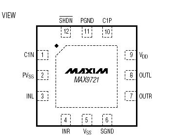 Specifications
SGND to PGND .....................................................-0.3V to +0.3V
VDD to SGND or PGND ............................................-0.3V to +2V
VSS to PVSS .........................................................-0.3V to +0.3V
C1P to PGND..............................................-0.3V to (VDD + 0.3V)
C1N to PGND............................................(PVSS - 0.3V) to +0.3V
VSS, PVSS to GND ...................................................+0.3V to -2V
OUTR, OUTL, INR, INL to SGND .......(VSS - 0.3V) to (VDD + 0.3V)
SHDN to SGND or PGND...........................................-0.3V to +4V
Output Short-Circuit Current ....................................Continuous
Continuous Power Dissipation (TA = +70°C)
12-Bump UCSP (derate 6.5mW/°C above 70°C).......518.8mW
12-Pin Thin QFN (derate 16.9mW/°C above 70°C)..1349.1mW
Junction Temperature....................................................+150°C
Operating Temperature Range ........................-40°C to +85°C
Storage Temperature Range .........................-65°C to +150°C
Bump Temperature (soldering) Reflow...........................+230°C
Lead Temperature (soldering, 10s) ...............................+300°C
Stresses beyond those listed under "Absolute Maximum Ratings" may cause permanent damage to the device. These are stress ratings only, and functional operation of the device at these or any other conditions beyond those indicated in the operational sections of the specifications is not implied. Exposure to absolute maximum rating conditions for extended periods may affect device reliability.
DescriptionThe MAX9721 fixed-gain, stereo headphone amplifier is ideal for portable equipment where board space is at a premium. The MAX9721 uses a unique, patented DirectDrive architecture to produce a ground-referenced output from a single supply, eliminating the need for large DC-blocking capacitors, saving cost, board space, and component height. Fixed gains of -2V/V (MAX9721A), -1.5V/V (MAX9721B), and -1V/V (MAX9721C) further reduce external component count.
The MAX9721 delivers up to 20mW per channel into a 32Ω load and achieves 0.006% THD+N. An 80dB at 1kHz power-supply rejection ratio (PSRR) allows the MAX9721 to operate from noisy digital supplies without an additional linear regulator. The MAX9721 includes ±8kV ESD protection on the headphone output. Comprehensive click-and-pop circuitry suppresses audible clicks and pops at startup and shutdown. A low-power shutdown mode reduces supply current to 1.0µA (typ).
The MAX9721 operates from a single 0.9V to 1.8V supply allowing the device to be powered directly from a single AA or AAA battery. The MAX9721 consumes only 2.2mA of supply current, provides short-circuit protection, and is specified over the extended -40°C to +85°C temperature range. The MAX9721 is available in a tiny (1.54mm x 2.02mm x 0.6mm), 12-bump chip-scale package (UCSP™) and a 12-pin thin QFN package (4mm x 4mm x 0.8mm).

 MAX9721 Data Sheet