SeekIC No. : 004414817
Detail
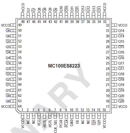
MC100ES8223: Features: • 1:22 differential clock fanout buffer• 50 ps maximum device skew1• SiGe technology• Supports DC to 800 MHz operation1 of clock or data signals• 1.5V HSTL co...
 MC100ES8223 Data Sheet
floor Price/Ceiling Price
- Part Number:
- MC100ES8223
- Supply Ability:
- 5000
Price Break
- Qty
- 1~5000
- Unit Price
- Negotiable
- Processing time
- 15 Days
SeekIC Buyer Protection PLUS - newly updated for 2013!
- Escrow Protection.
- Guaranteed refunds.
- Secure payments.
- Learn more >>
Month Sales
268 Transactions
Payment Methods
All payment methods are secure and covered by SeekIC Buyer Protection PLUS.
Notice: When you place an order, your payment is made to SeekIC and not to your seller. SeekIC only pays the seller after confirming you have received your order. We will also never share your payment details with your seller.