SeekIC No. : 004416321
Detail
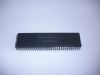
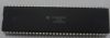
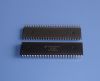
MC68340: Features: • High Functional Integration on a Single Piece of Silicon• CPU32-MC68020-Derived 32-Bit Central Processor Unit- Upward Object-Code Compatible with MC68000 and MC68010- Additio...
 MC68340 Data Sheet
floor Price/Ceiling Price
- Part Number:
- MC68340
- Supply Ability:
- 5000
Price Break
- Qty
- 1~5000
- Unit Price
- Negotiable
- Processing time
- 15 Days
SeekIC Buyer Protection PLUS - newly updated for 2013!
- Escrow Protection.
- Guaranteed refunds.
- Secure payments.
- Learn more >>
Month Sales
268 Transactions
Payment Methods
All payment methods are secure and covered by SeekIC Buyer Protection PLUS.
Notice: When you place an order, your payment is made to SeekIC and not to your seller. SeekIC only pays the seller after confirming you have received your order. We will also never share your payment details with your seller.