SeekIC No. : 004416562
Detail
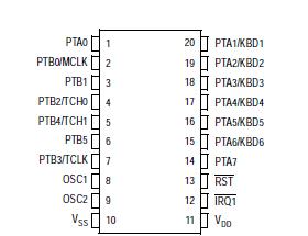
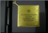
MC68HC908RK2: Features: • High-performance M68HC08 architecture• Fully upward-compatible object code with M6805, M146805, and M68HC05 Families• Maximum internal bus frequency of 4 MHz at 3.3 vol...
 MC68HC908RK2 Data Sheet
floor Price/Ceiling Price
- Part Number:
- MC68HC908RK2
- Supply Ability:
- 5000
Price Break
- Qty
- 1~5000
- Unit Price
- Negotiable
- Processing time
- 15 Days
SeekIC Buyer Protection PLUS - newly updated for 2013!
- Escrow Protection.
- Guaranteed refunds.
- Secure payments.
- Learn more >>
Month Sales
268 Transactions
Payment Methods
All payment methods are secure and covered by SeekIC Buyer Protection PLUS.
Notice: When you place an order, your payment is made to SeekIC and not to your seller. SeekIC only pays the seller after confirming you have received your order. We will also never share your payment details with your seller.