Number of Gates
: 4
Maximum Operating Temperature
: + 125 C
Mounting Style
: SMD/SMT
Packaging
: Reel
Package / Case
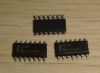
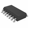
: SOIC-14
Product
: NOR
Supply Voltage - Min
: 2 V
Supply Voltage - Max
: 6 V
High Level Output Current
: - 5.2 mA
Low Level Output Current
: 5.2 mA
Logic Family
: HC
Number of Lines (Input / Output)
: 2-IN / 1
Propagation Delay Time
: 75 ns at 2 V, 30 ns at 3 V, 15 ns at 4.5 V, 13 ns at 6 V
DescriptionThe MC74HC02ADR2G is one member of the MC74HC02A series.The MC74HC02A is identical in pinout to the LS02. The device inputs are compatible with standard CMOS outputs; with pullup resistors, they are compatible with LSTTL outputs.SCILLC reserves the right to make changes without further notice to any products herein. SCILLC makes no warranty, representation or guarantee regarding the suitability of its products for any particular purpose, nor does SCILLC assume any liability arising out of the application or use of any product or circuit, and specifically disclaims any and all liability, including without limitation special, consequential or incidental damages."Typical" parameters which may be provided in SCILLC data sheets and/or specifications can and do vary in different applications and actual performance may vary over time.
Features of the MC74HC02ADR2G are:(1)output drive capability: 10 LSTTL Loads; (2)outputs directly interface to CMOS, NMOS, and TTL; (3)operating voltage range: 2.0 to 6.0 V; (4)low input current: 1.0A; (5)high noise immunity characteristic of CMOS devices; (6)in compliance with the requirements defined by JEDEC standard no. 7.0 A; (7)chip complexity: 40 FETs or 10 equivalent gates; (8)pb-free packages are available.
The absolute maximum ratings of the MC74HC02ADR2G can be summarized as:(1)storage temperature range:-65 to 150;(2)lead temperature range:260;(3)DC supply voltage (referenced to GND):-0.5 to 7.0V;(4)DC input voltage (referenced to GND):-0.5 to Vcc+0.5V;(5)power dissipation:1W;(6)DC output current, per pin:±25mA;(7)DC output voltage (referenced to GND):-0.5 to Vcc+0.5V;(8)DC input current, per pin:±20mA.Stresses exceeding Maximum Ratings may damage the device. Maximum Ratings are stress ratings only. Functional operation above the Recommended Operating Conditions is not implied. Extended exposure to stresses above the Recommended Operating Conditions may affect device reliability.This device contains protection circuitry to guard against damage due to high static voltages or electric fields. However, precautions must be taken to avoid applications of any voltage higher than maximum rated voltages to this high-impedance circuit. For proper operation, V;n and Vout should be constrained to the range GND (Vin or Vout) Vcc.Unused inputs must always be tied to an appropriate logic voltage level (e.g.,either GND or Vac).Unused outputs must be left open.
Parameters: | Technical/Catalog Information | MC74HC02ADR2G |
| Vendor | ON Semiconductor |
| Category | Integrated Circuits (ICs) |
| Number of Circuits | 4 - Quad |
| Package / Case | 14-SOIC (3.9mm Width), 14-SOL |
| Logic Type | NOR Gate |
| Packaging | Tape & Reel (TR) |
| Mounting Type | Surface Mount |
| Number of Inputs | 2 |
| Current - Output High, Low | 5.2mA, 5.2mA |
| Supply Voltage | 2 V ~ 6 V |
| Operating Temperature | -55°C ~ 125°C |
| Voltage - Supply | 2 V ~ 6 V |
| Drawing Number | * |
| Lead Free Status | Lead Free |
| RoHS Status | RoHS Compliant |
| Other Names | MC74HC02ADR2G
MC74HC02ADR2G
MC74HC02ADR2GOSTR ND
MC74HC02ADR2GOSTRND
MC74HC02ADR2GOSTR
|

 MC74HC02ADR2G Data Sheet