Series: -
PLL: Yes
Number of Circuits: 1
Differential - Input:Output: No/No
Mounting Type: Surface Mount
Packaging: Tube
Divider/Multiplier: Yes/Yes
Operating Temperature: 0°C ~ 70°C
Frequency - Max: 100MHz
Input: TTL
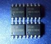
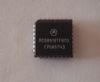
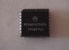
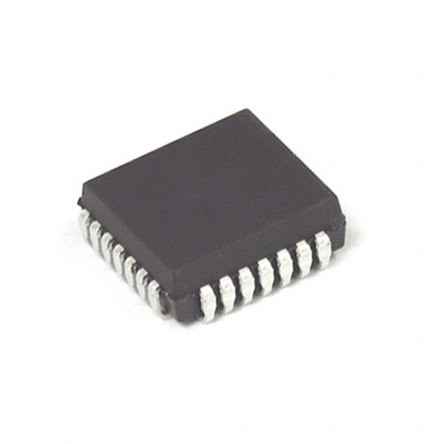
Package / Case: 28-LCC (J-Lead)
Output: CMOS, TTL
Voltage - Supply: 4.75 V ~ 5.25 V
Ratio - Input:Output: 3:8
Type: Clock Driver, Fanout Distribution, Multiplexer
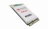
Manufacturer: Freescale Semiconductor
Supplier Device Package: 28-PLCC (12.45x12.45)
Features: • Five Outputs (Q0Q4) with OutputOutput Skew < 500 ps each being phase and frequency locked to the
SYNC input
• The phase variation from parttopart between the SYNC and FEEDBACK inputs is less than 550 ps (derived
from the tPD specification, which defines the parttopart skew)
• Input/Output phaselocked frequency ratios of 1:2, 1:1, and 2:1 are available
• Input frequency range from 5MHz 2X_Q FMAX spec. (10MHz 2X_Q FMAX for the TFN133 version)
• Additional outputs available at 2X and +2 the system "Q" frequency. Also a Q(180° phase shift) output available
• All outputs have ±36 mA drive (equal high and low) at CMOS levels, and can drive either CMOS or TTL inputs.
All inputs are TTLlevel compatible. ±88mA IOL/IOH specifications guarantee 50 transmission line switching
on the incident edge
• Test Mode pin (PLL_EN) provided for low frequency testing. Two selectable CLOCK inputs for test or
redundancy purposes. All outputs can go into high impedance (3state) for board test purposes
• Lock Indicator (LOCK) accuracy indicates a phaselocked state
Application1. Several specifications can only be measured when the MC88915TFN55, 70 and 100 are in phaselocked operation. It is not possible to have the part in phaselock on ATE (automated test equipment). Statistical characterization techniques were used to guarantee those specifications which cannot be measured on the ATE. MC88915TFN55, 70 and 100 units were fabricated with key transistor properties intentionally varied to create a 14 cell designed experimental matrix. IC performance was characterized over a range of transistor properties (represented by the 14 cells) in excess of the expected process variation of the wafer fabrication area, to set performance limits of ATE testable specifications within those which are to be guaranteed by statistical characterization. In this way all units passing the ATE test will meet or exceed the nontested specifications limits.
2. These two specs (tRlSE/FALL and tPULSE Width 2X_Q output) guarantee that the MC88915T meets the 40MHz
and 33MHz MC68040 PClock input specification (at 80MHz and 66MHz, respectively). For these two specs to
be guaranteed by Motorola, the termination scheme shown below in Figure 1 must be used.
3. The wiring Diagrams and explanations in Figure 5 demonstrate the input and output frequency relationships
for three possible feedback configurations. The allowable SYNC input range for each case is also indicated. There
are two allowable SYNC frequency ranges, depending whether FREQ_SEL is high or low. Although not shown, it
is possible to feed back the Q5 output, thus creating a 180° phase shift between the SYNC input and the "Q"
outputs. Table 1 below summarizes the allowable SYNC frequency range for each possible configuration.
Pinout Description
The MC88915T Clock Driver utilizes phaselocked loop technology to lock its low skew outputs' frequency and phase onto an input reference clock. It is designed to provide clock distribution for high performance PC's and workstations. For a 3.3V version, see the MC88LV915T data sheet
The PLL MC88915TFN100 allows the high current, low skew outputs to lock onto a single clock input and distribute MC88915TFN100 with essentially zero delay to multiple components on a board. The PLL also allows the MC88915T to multiply a low frequency input clock and distribute MC88915TFN100 locally at a higher (2X) system frequency. Multiple 88915's can lock onto a single reference clock, which is ideal for applications when a central system clock must be distributed synchronously to multiple boards (see Figure 7).
Five "Q" outputs (Q0Q4) are provided with less than 500 ps skew between their rising edges. The Q5 output is inverted (180° phase shift) from the "Q" outputs. The 2X_Q output runs at twice the "Q" output frequency, while the Q/2 runs at 1/2 the "Q" frequency.
The VCO MC88915TFN100 is designed to run optimally between 20 MHz and the 2X_Q Fmax specification. The wiring diagrams in
Figure 5 detail the different feedback configurations which create specific input/output frequency relationships. Possible frequency ratios of the "Q" outputs to the SYNC input are 2:1, 1:1, and 1:2.
The FREQ_SEL MC88915TFN100 pin provides one bit programmable divideby in the feedback path of the PLL. IMC88915TFN100 selects between divideby1 and divideby2 of the VCO before iMC88915TFN100 signal reaches the internal clock distribution section of the chip (see the block diagram on page 2). In most applications FREQ_SEL should be held high (÷1). If a low frequency reference clock input is used, holding FREQ_SEL low (÷2) will allow the VCO to run in its optimal range (>20MHz and >40MHz for the TFN133 version).
In normal phaselocked operation the PLL_EN pin is held high. Pulling the PLL_EN pin low disables the VCO and puts the 88915 in a static "test mode". In MC88915TFN100 there is no frequency limitation on the input clock, which is necessary for a low frequency board test environment. The second SYNC input can be used as a test clock input to further simplify boardlevel testing (see detailed description on page 11)
Pulling the OE /RST pin low puts the clock outputs 2X_Q, Q0Q4, Q5 and Q/2 into a high impedance state (3state). After the OE /RST pin goes back high Q0Q4, Q5 and Q/2 will be reset in the low state, with 2X_Q being the inverse of the selected SYNC input. Assuming PLL_EN is low, the outputs will remain reset until the 88915 sees a SYNC input pulse.
A lock indicator output (LOCK) will go high when the loop is in steadystate phase and frequency lock. The LOCK output will go low if phaselock is lost or when the PLL_EN pin is low. The LOCK output will go high no later than 10ms after the 88915 sees a SYNC signal and full 5V VCC.
Parameters: | Technical/Catalog Information | MC88915TFN100 |
| Vendor | Freescale Semiconductor |
| Category | Integrated Circuits (ICs) |
| Type | PLL Clock Driver |
| Voltage - Supply | 4.75 V ~ 5.25 V |
| Number of Outputs | 8 |
| Input | TTL |
| Output | CMOS, TTL |
| Frequency-Max | 100MHz |
| Package / Case | 28-PLCC |
| Packaging | Tube |
| Operating Temperature | 0°C ~ 70°C |
| Drawing Number | 375; 776-02; FN; 28 |
| Lead Free Status | Contains Lead |
| RoHS Status | RoHS Non-Compliant |
| Other Names | MC88915TFN100
MC88915TFN100
|
 MC88915TFN100 Data Sheet