SeekIC No. : 004417406
Detail
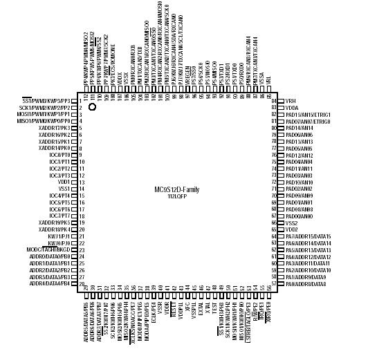
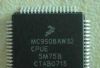
MC9S12D: Features: Not all features listed here are available in all configurations.Additional information about D and B family inter-operability is given in:EB386 HCS12 D-Family Compatibility Consideration...
 MC9S12D Data Sheet
floor Price/Ceiling Price
- Part Number:
- MC9S12D
- Supply Ability:
- 5000
Price Break
- Qty
- 1~5000
- Unit Price
- Negotiable
- Processing time
- 15 Days
SeekIC Buyer Protection PLUS - newly updated for 2013!
- Escrow Protection.
- Guaranteed refunds.
- Secure payments.
- Learn more >>
Month Sales
268 Transactions
Payment Methods
All payment methods are secure and covered by SeekIC Buyer Protection PLUS.
Notice: When you place an order, your payment is made to SeekIC and not to your seller. SeekIC only pays the seller after confirming you have received your order. We will also never share your payment details with your seller.