MMC2107

Features: ` Selects the chip operating mode: Master mode Single-chip mode Emulation mode Factory access slave test (FAST) mode for factory test only` Selects external clock or phase-lock loop (PLL) mode with internal or external reference` Selects output pad strength` Selects boot device` Sele...

product image

MMC2107 Picture
SeekIC No. : 004423732 Detail

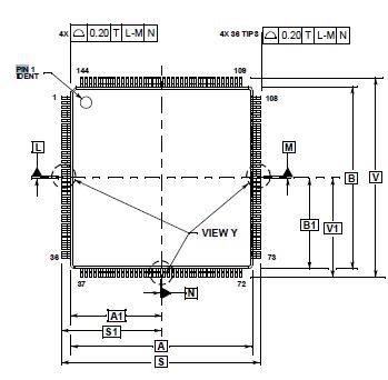
MMC2107: Features: ` Selects the chip operating mode: Master mode Single-chip mode Emulation mode Factory access slave test (FAST) mode for factory test only` Selects external clock or phase-lock loop (P...

floor Price/Ceiling Price

Part Number:
MMC2107
Supply Ability:
5000

Price Break

  • Qty
  • 1~5000
  • Unit Price
  • Negotiable
  • Processing time
  • 15 Days
Total Cost: $ 0.00

SeekIC Buyer Protection PLUS - newly updated for 2013!

  • Escrow Protection.
  • Guaranteed refunds.
  • Secure payments.
  • Learn more >>

Month Sales

268 Transactions

Rating

evaluate  (4.8 stars)

Upload time: 2024/4/28

Payment Methods

All payment methods are secure and covered by SeekIC Buyer Protection PLUS.

Notice: When you place an order, your payment is made to SeekIC and not to your seller. SeekIC only pays the seller after confirming you have received your order. We will also never share your payment details with your seller.
Product Details

Description


Features:

` Selects the chip operating mode:
   Master mode
   Single-chip mode
   Emulation mode
   Factory access slave test (FAST) mode for factory test only
` Selects external clock or phase-lock loop (PLL) mode with internal or external reference
` Selects output pad strength
` Selects boot device
` Selects module configuration
` Selects bus monitor configuration


Pinout

  Connection Diagram


Specifications

Parameter

Symbol

Value

Unit

Supply voltage

VDD

0.3 to +4.0

V

Clock synthesizer supply voltage

VDDSYN

0.3 to +4.0

V

RAM memory standby supply voltage

VSTBY

0.3 to +4.0

V

FLASH memory supply voltage

VDDF

0.3 to +4.0

V

FLASH memory program/erase supply voltage

VPP

0.3 to + 6.0

V

Analog supply voltage

VDDA

0.3 to + 6.0

V

Analog reference supply voltage

VRH

0.3 to + 6.0

V

Analog ESD protection voltage

VDDH

0.3 to + 6.0

V

Digital input voltage(1)

VIN

0.3 to + 4.0

V

Analog input voltage

VAIN

0.3 to + 6.0

V

Instantaneous maximum current single pin limit
(applies to all pins)(2), (3)

ID

25

mA

Operating temperature range (packaged)

TA
(TL to TH)

40 to 85

Storage temperature range

TSTG

65 to 150


1. Input must be current limited to the value specified. To determine the value of the required current-limiting resistor, calculate resistance values for positive and negative clamp voltages, then use the larger of the two values.
2. All functional non-supply pins are internally clamped to VSS and VDD.
3. Power supply must maintain regulation within operating VDD range during instantaneous and operating maximum current conditions. If positive injection current (Vin > VDD) is greater than IDD, the injection current may flow out of VDD and could result in external power supply going out of regulation. Ensure external VDD load will shunt current greater than maximum injection current. This will be the greatest risk when the MCU is not consuming power (ex; no clock).


Customers Who Bought This Item Also Bought

Margin,quality,low-cost products with low minimum orders. Secure your online payments with SeekIC Buyer Protection.
Fans, Thermal Management
Potentiometers, Variable Resistors
Undefined Category
Soldering, Desoldering, Rework Products
Isolators
Motors, Solenoids, Driver Boards/Modules
View more