MNCLC401A-X

Features: ·-3dB bandwidth of 150MHz·0.1% settling in 10ns·Low power, 150mW·Overload and short circuit protected·Stable without compensation·Recommended gain range +7 to +50·CONTROLLING DOCUMENT: CLC401AJ-QML 5962-8997301PAApplication·Flash, precision A/D conversion·Photodiode, CCD preamps·IF proce...

product image

MNCLC401A-X Picture
SeekIC No. : 004424742 Detail

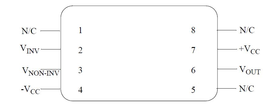
MNCLC401A-X: Features: ·-3dB bandwidth of 150MHz·0.1% settling in 10ns·Low power, 150mW·Overload and short circuit protected·Stable without compensation·Recommended gain range +7 to +50·CONTROLLING DOCUMENT: CLC...

floor Price/Ceiling Price

Part Number:
MNCLC401A-X
Supply Ability:
5000

Price Break

  • Qty
  • 1~5000
  • Unit Price
  • Negotiable
  • Processing time
  • 15 Days
Total Cost: $ 0.00

SeekIC Buyer Protection PLUS - newly updated for 2013!

  • Escrow Protection.
  • Guaranteed refunds.
  • Secure payments.
  • Learn more >>

Month Sales

268 Transactions

Rating

evaluate  (4.8 stars)

Upload time: 2024/4/28

Payment Methods

All payment methods are secure and covered by SeekIC Buyer Protection PLUS.

Notice: When you place an order, your payment is made to SeekIC and not to your seller. SeekIC only pays the seller after confirming you have received your order. We will also never share your payment details with your seller.
Product Details

Description


Features:

· -3dB bandwidth of 150MHz
· 0.1% settling in 10ns
· Low power, 150mW
· Overload and short circuit protected
· Stable without compensation
· Recommended gain range +7 to +50
· CONTROLLING DOCUMENT: CLC401AJ-QML 5962-8997301PA


Application

· Flash, precision A/D conversion
· Photodiode, CCD preamps
· IF processors
· High-speed modems, radios
· Line drivers
· DC-coupled log ampifiers
· High-speed communications


Pinout

  Connection Diagram


Specifications

Supply Voltage (Vs)..............................................+7V dc
Output Current (Iout)..........................................+70mA
Maximum Power Dissipation (Pd)
(Note 2)..................................................................1.2W
Junction Temperature (Tj)...................................+175 C
Storage Temperature Range.................-65 C to +150 C
Lead Temperature (soldering, 10 seconds).........+300 C
Thermal Resistance
Junction-to-ambient (ThetaJA)
Ceramic DIP (Still Air) ........................................134 C/W
(500 LFPM) ..........................................................80 C/W
Junction-to-case (ThetaJC)
Ceramic DIP ........................................................27 C/W
Package Weight
(typical)
Ceramic DIP .............................................................TBD
ESD Tolerance
(Note 3)
ESD Rating ..........................................................1000 V
Note 1: Absolute Maximum Ratings are limits beyond which damage to the device may occur. Operating Ratings are conditions for which the device is functional, but do not guarantee specific performance limits. For guaranteed specifications and test conditions see the Electrical Characteristics. The guaranteed specifications apply only for the test conditions listed. Some performance characteristics may degrade when the device is not operated under the listed test conditions.
Note 2: The maximum power dissipation must be derated at elevated temperatures and is dictated by Tjmax (maximum junction temperature), ThetaJA (package junction to ambient thermal resistance), and TA (ambient temperature). The maximum allowable power dissipation at any temperature is Pdmax = (Tjmax - TA)/ThetaJA or the number given in the Absolute Maximum Ratings, whichever is lower.
Note 3: Human body model, 100pF discharged through 1.5K Ohms.


Description

The CLC401 is a wideband, fast-settling operational amplifier designed for applications requiring a gain greater than +7. Constructed using an advanced complementary bipolar process and a proprietary design, the CLC401 features dynamic performance far beyond that of typical high-speed monolithic operational amplifiers. For example, at a gain of +20 V/V, the -3dB bandwidth is 150MHz and the rise/fall time is only 2.5ns.

The wide bandwidth and linear phase (0.2 deviation from linear at 50MHz) and a very flat gain response makes the CLC401 ideal for many digital communication system applications. For example, demodulators need both DC coupling and high-frequency amplification - requirements that are ordinarily difficult to meet.

The very fast 10ns settling to 0.1% and the ability to drive capacitive loads lend themselves well to flash A/D applications. Systems employing D/A converters also benefit from the settling time and also by the fact that current-to-voltage transimpedance amplification is easily accomplished. The CLC401 provides a quick, effective design solution. Its stable operation over the entire +7 to +50 gain range precludes the need for external compensation. And, unlike many other high-speed op amps, the CLC401's power dissipation of 150mW is compatible with designs which must limit total power dissipation or power supply requirements.


Customers Who Bought This Item Also Bought

Margin,quality,low-cost products with low minimum orders. Secure your online payments with SeekIC Buyer Protection.
Inductors, Coils, Chokes
Test Equipment
Optoelectronics
Prototyping Products
DE1
Cable Assemblies
Soldering, Desoldering, Rework Products
View more