MNCLC409A-X

Features: ·350MHz small signal bandwidth·-65/-72dBc 2nd/3rd harmonics (20MHz)·Low Noise·8ns settling to 0.1%·1200V/us slew rate·13.5mA supply current (+5V)·70mA output currentApplication·Flash A/D driver·D/A transimpedance buffer·Wide dynamic range IF amp·Radar/communication receivers·DDS post-amp...

product image

MNCLC409A-X Picture
SeekIC No. : 004424743 Detail

MNCLC409A-X: Features: ·350MHz small signal bandwidth·-65/-72dBc 2nd/3rd harmonics (20MHz)·Low Noise·8ns settling to 0.1%·1200V/us slew rate·13.5mA supply current (+5V)·70mA output currentApplication·Flash A/D d...

floor Price/Ceiling Price

Part Number:
MNCLC409A-X
Supply Ability:
5000

Price Break

  • Qty
  • 1~5000
  • Unit Price
  • Negotiable
  • Processing time
  • 15 Days
Total Cost: $ 0.00

SeekIC Buyer Protection PLUS - newly updated for 2013!

  • Escrow Protection.
  • Guaranteed refunds.
  • Secure payments.
  • Learn more >>

Month Sales

268 Transactions

Rating

evaluate  (4.8 stars)

Upload time: 2024/4/27

Payment Methods

All payment methods are secure and covered by SeekIC Buyer Protection PLUS.

Notice: When you place an order, your payment is made to SeekIC and not to your seller. SeekIC only pays the seller after confirming you have received your order. We will also never share your payment details with your seller.
Product Details

Description


Features:

· 350MHz small signal bandwidth
· -65/-72dBc 2nd/3rd harmonics (20MHz)
· Low Noise
· 8ns settling to 0.1%
· 1200V/us slew rate
· 13.5mA supply current (+5V)
· 70mA output current


Application

 ·Flash A/D driver
· D/A transimpedance buffer
· Wide dynamic range IF amp
· Radar/communication receivers
· DDS post-amps
· Wideband inverting summer
· Line driver


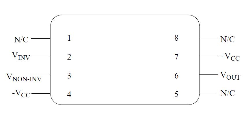
Pinout

  Connection Diagram


Specifications

Supply Voltage (Vcc)..............................................+7V dc
Common Mode Input Voltage (Vcm)..........................+Vcc
Differential Input Voltage.....................................+10V dc
Output Current (Io)...............................................+70mA
Power Dissipation (Pd)
(Note 2)....................................................................1.2W
Junction Temperature (Tj).....................................+175 C
Lead Temperature (soldering, 10 seconds)..........+300 C
Storage Temperature Range...................-65 C to +125 C
Thermal Resistance
ThetaJA (Junction to Ambient)
CERAMIC DIP (Still Air) ......................................132 C/W
(500 LFPM) .........................................................77 C/W
LCC (Still Air) ......................................................97 C/W
(500 LFPM) .........................................................67 C/W
ThetaJC (Junction to Case)
CERAMIC DIP ......................................................26 C/W
LCC ....................................................................27 C/W
Package Weight
(Typical)
CERAMIC DIP ....................................................1070 mg
LCC .....................................................................465 mg
ESD Tolerance
(Note 3)
ESD Rating ............................................................500 V
Note 1: Absolute Maximum Ratings are limits beyond which damage to the device may occur. Operating Ratings are conditions for which the device is functional, but do not guarantee specific performance limits. For guaranteed specifications and test conditions see the Electrical Characteristics. The guaranteed specifications apply only for the test conditions listed. Some performance characteristics may degrade when the device is not operated under the listed test conditions.
Note 2: The maximum power dissipation must be derated at elevated temperatures and is dictated by Tjmax (maximum junction temperature), ThetaJA (package junction to ambient thermal resistance, and TA (ambient temperature). The maximum allowable power dissipation at any temperature is Pdmax = (Tjmax - TA)/ThetaJA or the number given in the Absolute Maximum Ratings, whichever is lower.
Note 3: Human body model, 1.5K Ohms in series with 100pF.


Description

The CLC409 is a very wideband, DC coupled monolithic operational amplifier designed specifically for wide dynamic range systems requiring exceptional signal fidelity. Benefiting from Comlinear's current feedback architecture, the CLC409 offers a gain range of +1 to +10 while providing stable, oscillation free operation without external compensation, even at unity gain.

With its 350MHz small signal bandwidth (Vout = 2Vpp), 10-bit distortion levels through 20MHz (Rl = 100Ohms), 8-bit distortion levels through 60Mhz, 2.2nV/SqRtHz input referred noise and 13.5mA supply current, the CLC409 is the ideal driver or buffer for high speed flash A/D and D/A converters.

Wide dynamic range systems such as radar and communication receivers requiring a wideband amplifier offering exceptional signal purity will find the CLC409's low input referred noise and low harmonic and intermodulation distortion make it an attractive high speed solution.


Customers Who Bought This Item Also Bought

Margin,quality,low-cost products with low minimum orders. Secure your online payments with SeekIC Buyer Protection.
Hardware, Fasteners, Accessories
Industrial Controls, Meters
Memory Cards, Modules
Potentiometers, Variable Resistors
LED Products
Circuit Protection
View more