Features: · -3dB bandwidth of 200MHz
· 0.05% settling in 12ns
· Low power, 160mW (40mW disabled)
· Low distortion, -60dBc at 20MHz
· Fast disable (200ns)
· Differential gain/phase: 0.01%/0.01 deg
· +1 to +8 closed-loop gain rangeApplication· Video switching and distribution
· Analog bus driving (with disable)
· Low power "standby" using disable
· Fast, precision A/D conversion
· D/A current-to-voltage conversion
· IF processors
· High-speed communicationsPinout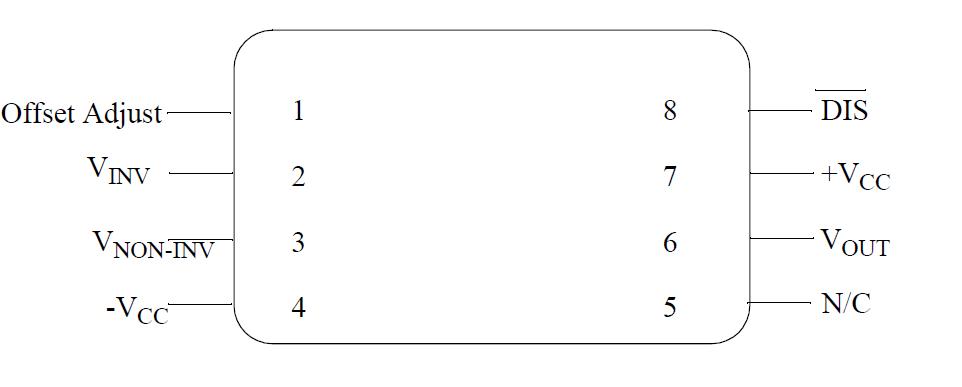 Specifications
Supply Voltage (Vs)............................................+7V dc
Output Current (Iout)..........................................70mA
Common Mode Input Voltage (Vcm)........................+Vs
Differential Input Voltage (Vid).................................5V
Disable Input Voltage (D I S pin).............................+Vs
Applied Output Voltage when Disabled...................+Vs
Maximum Power Dissipation (Pd)
(Note 2)................................................................1.2W
Lead Temperature (soldering, 10 seconds)......+300 C
Junction Temperature (Tj).................................+175 C
Storage Temperature..........................-65 C to +150 C
Thermal Resistance
Junction -to-ambient (ThetaJA)
Ceramic DIP (Still Air) .............................................TBD
(500 LFPM)
Junction -to-case (ThetaJC)
Ceramic DIP ...........................................................TBD
Package Weight
(Typical)
Ceramic DIP ...........................................................TBD
ESD Tolerance
(Note 3)
ESD Rating ........................................................1000V
Note 1: Absolute Maximum Ratings are limits beyond which damage to the device may occur. Operating Ratings are conditions for which the device is functional, but do not guarantee specific performance limits. For guaranteed specifications and test conditions see the Electrical Characteristics. The guaranteed specifications apply only for the test conditions listed. Some performance characteristics may degrade when the device is not operated under the listed test conditions.
Note 2: The maximum power dissipation must be derated at elevated temperatures and is dictated by Tjmax (maximum junction temperature), ThetaJA (package junction to ambient thermal resistance), and TA (ambient temperature). The maximum allowable power dissipation at any temperature is Pdmax = (Tjmax - TA) / ThetaJA or the number given in the Absolute Maximum Ratings, whichever is lower.
Note 3: Human body model, 100pF discharged through 1.5K Ohms.
DescriptionThe current-feedback CLC410 is a fast-settling, wideband, monolithic op amp with fast disable/enable feature. Designed for low-gain applications (Av = +1 to +8), the CLC410 consumes only 160mW of power (180mW max) yet provides a -3dB bandwidth of 200MHz (Av = +2) and 0.05% settling in 12ns (15ns max). Plus, the disable feature provides fast turn-on (100ns) and turn-off (200ns). In addition, the CLC410 offers both high performance and stability without compensation, even at a gain of +1.
The CLC410 provides a simple, high-performance solution for video switching and distribution applications, especially where analog buses benefit from use of the disable function to "multiplex" signals onto the bus. Differential gain/phase of 0.01%/0.01 provide high fidelity and the 70mA output current offers ample drive capability. The CLC410's fast settling, low distortion, and high drive capabilities make it an ideal ADC driver. The low 160mW quiescent power consumption and very low 40mW disabled power consumption suggest use where power is critical and/or "system off" power consumption must be minimized.

 MNCLC410A-X Data Sheet


