MRF21045LSR3

Transistors RF MOSFET Power RF PWR LDMOS NI400LS

product image

MRF21045LSR3 Picture
SeekIC No. : 00220356 Detail

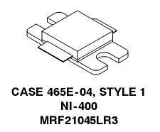
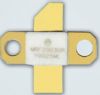
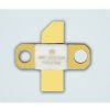
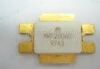
MRF21045LSR3: Transistors RF MOSFET Power RF PWR LDMOS NI400LS

floor Price/Ceiling Price

Part Number:
MRF21045LSR3
Mfg:
Freescale Semiconductor
Supply Ability:
5000

Price Break

  • Qty
  • 1~5000
  • Unit Price
  • Negotiable
  • Processing time
  • 15 Days
Total Cost: $ 0.00

SeekIC Buyer Protection PLUS - newly updated for 2013!

  • Escrow Protection.
  • Guaranteed refunds.
  • Secure payments.
  • Learn more >>

Month Sales

268 Transactions

Rating

evaluate  (4.8 stars)

Upload time: 2024/4/24

Payment Methods

All payment methods are secure and covered by SeekIC Buyer Protection PLUS.

Notice: When you place an order, your payment is made to SeekIC and not to your seller. SeekIC only pays the seller after confirming you have received your order. We will also never share your payment details with your seller.
Product Details

Quick Details

Configuration : Single Transistor Polarity : N-Channel
Frequency : 2.11 GHz to 2.17 GHz Gain : 15 dB
Output Power : 10 W Drain-Source Breakdown Voltage : 65 V
Gate-Source Breakdown Voltage : - 0.5 V, + 15 V Maximum Operating Temperature : + 150 C
Package / Case : NI-400S-3 Packaging : Reel    

Description

Continuous Drain Current :
Configuration : Single
Transistor Polarity : N-Channel
Maximum Operating Temperature : + 150 C
Packaging : Reel
Drain-Source Breakdown Voltage : 65 V
Gain : 15 dB
Frequency : 2.11 GHz to 2.17 GHz
Output Power : 10 W
Gate-Source Breakdown Voltage : - 0.5 V, + 15 V
Package / Case : NI-400S-3


Application

Typical 2-carrier W-CDMA Performance for VDD = 28 Volts, IDQ = 500 mA,
   f1 = 2135 MHz, f2 = 2145 MHz, Channel Bandwidth = 3.84 MHz,
   Adjacent Channels measured over 3.84 MHz Bandwidth at  f1 -5 MHz
   and f2 +5 MHz, Distortion Products measured over a 3.84 MHz Bandwidth
   at f1 -10 MHz and f2 +10 MHz, Peak/Avg. = 8.3 dB @ 0.01% Probability on CCDF.
   Output Power ó 10 Watts Avg.
   Efficiency ó 23.5%
   Gain ó 15 dB
   IM3 ó -37.5 dBc
   ACPR ó -41 dBc
Internally Matched, Controlled Q, for Ease of Use
High Gain, High Efficiency and High Linearity
Integrated ESD Protection
Designed for Maximum Gain and Insertion Phase Flatness
Capable of Handling 5:1 VSWR, @ 28 Vdc, 2170 MHz, 45 Watts CW
   Output Power
Excellent Thermal Stability
Characterized with Series Equivalent Large-Signal Impedance Parameters
Low Gold Plating Thickness on Leads, 40 Nominal.
In Tape and Reel. R3 Suffix = 250 Units per 32 mm, 13 Inch Reel.


Pinout

  Connection Diagram


Specifications

Rating Symbol Value Unit
Drain-Source Voltage VDSS 65 Vdc
Gate-Source Voltage VGS -0.5, +15 Vdc
Total Device Dissipation @ TC = 25°C
Derate above 25°C
PD 105
0.60
Watts
W/°C
Storage Temperature Range Tstg -65 to +150 °C
Operating Junction Temperature TJ 200 °C


Customers Who Bought This Item Also Bought

Margin,quality,low-cost products with low minimum orders. Secure your online payments with SeekIC Buyer Protection.
Boxes, Enclosures, Racks
Transformers
Cables, Wires
Circuit Protection
Optoelectronics
Computers, Office - Components, Accessories
View more