Operating Temperature Range
:
Core
: MSP430
Data Bus Width
: 16 bit
On-Chip ADC
: Yes
Operating Supply Voltage
: 1.8 V to 3.6 V
Mounting Style
: SMD/SMT
Maximum Clock Frequency
: 16 MHz
Program Memory Size
: 8 KB
Data RAM Size
: 256 B
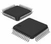
Package / Case
: LQFP-64
Processor Series
: 4 Series
Features: ` Low Supply-Voltage Range, 1.8 V to 3.6 V
` Ultralow-Power Consumption:
− Active Mode: 200 A at 1 MHz, 2.2 V
− Standby Mode: 0.7 A
− Off Mode (RAM Retention): 0.1 A
` Five Power-Saving Modes
` Wake-Up From Standby Mode in Less
Than 6 s
` Frequency-Locked Loop, FLL+
` 16-Bit RISC Architecture, 125-ns
Instruction Cycle Time
` Scan IF for Background Water, Heat, and
Gas Volume Measurement
` 16-Bit Timer_A With Three
Capture/Compare Registers
` 16-Bit Timer_A With Five
Capture/Compare Registers
` Integrated LCD Driver for Up to
96 Segments
` On-Chip Comparator
` Serial Onboard Programming,
No External Programming Voltage Needed
Programmable Code Protection by Security Fuse
` Brownout Detector
` Supply Voltage Supervisor/Monitor With
Programmable Level Detection
` Bootstrap Loader in Flash Devices
` Family Members Include:
− MSP430FW423:
8KB + 256B Flash Memory,
256B RAM
− MSP430FW425:
16KB + 256B Flash Memory,
512B RAM
− MSP430FW427:
32KB + 256B Flash Memory,
1KB RAM
` Available in 64-Pin Quad Flat Pack (QFP)
` For Complete Module Descriptions, Refer
to the MSP430x4xx Family User's Guide,
Literature Number SLAU056Pinout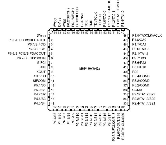 SpecificationsVoltage applied at VCC to VSS . . . . . . . . . . . . . . . . . . . . . . . . . . . . . . . . . . . . . . . . . . . . . . . . . . −0.3 V to + 4.1 V
Voltage applied to any pin (see Note) . . . . . . . . . . . . . . . . . . . . . . . . . . . . . . . . . . . . . . . . −0.3 V to VCC + 0.3 V
Diode current at any device terminal . . . . . . . . . . . . . . . . . . . . . . . . . . . . . . . . . . . . . . . . . . . . . . . . . . . . . .±2 mA
Storage temperature (unprogrammed device) . . . . . . . . . . . . . . . . . . . . . . . . . . . . . . . . . . . . . . . −55°C to 150°C
Storage temperature (programmed device) . . . . . . . . . . . . . . . . . . . . . . . . . . . . . . . . . . . . . . . . . . −40°C to 85°C
† Stresses beyond those listed under "absolute maximum ratings" may cause permanent damage to the device. These are stress ratings only, and
functional operation of the device at these or any other conditions beyond those indicated under "recommended operating conditions" is not
implied. Exposure to absolute-maximum-rated conditions for extended periods may affect device reliability.
NOTE: All voltages referenced to VSS. The JTAG fuse-blow voltage, VFB, is allowed to exceed the absolute maximum rating. The voltage is
applied to the TDI/TCLK pin when blowing the JTAG fuse.DescriptionThe Texas Instruments MSP430FW423IPM ultralow-power microcontrollers consists of several devices featuring different sets of peripherals targeted for various applications. The architecture, combined with five low power modes, is optimized to achieve extended battery life in portable measurement applications. The MSP430FW423IPM features a powerful 16-bit RISC CPU, 16-bit registers, and constant generators that contribute to maximum code efficiency. The digitally controlled oscillator (DCO) of MSP430FW423IPM allows wake-up from low-power modes to active mode in less than 6 s.
The MSP430FW423IPM series are microcontroller configurations with two built-in 16-bit timers, a comparator, 96 LCD segment drive capability, a scan interface, and 48 I/O pins. Typical applications for MSP430FW423IPM include sensor systems that capture analog signals, convert them to digital values, and process the data and transmit them to a host system. The comparator and timers of MSP430FW423IPM make the configurations ideal for gas, heat, and water meters, industrial meters, counter applications, handheld meters, etc.
Parameters: | Technical/Catalog Information | MSP430FW423IPM |
| Vendor | Texas Instruments |
| Category | Integrated Circuits (ICs) |
| Program Memory Size | 8KB (8K x 8 + 256B) |
| RAM Size | 256 x 8 |
| Number of I /O | 48 |
| Package / Case | 64-LQFP |
| Speed | 8MHz |
| Controller Series | MSP430 |
| Oscillator Type | Internal |
| Packaging | Tray |
| Program Memory Type | FLASH |
| EEPROM Size | - |
| Core Processor | RISC |
| Data Converters | Slope A/D |
| Core Size | 16-Bit |
| Operating Temperature | -40°C ~ 85°C |
| Connectivity | - |
| Peripherals | Brown-out Detect/Reset, LCD, POR, PWM, WDT |
| Voltage - Supply (Vcc/Vdd) | 1.8 V ~ 3.6 V |
| Drawing Number | 296; 4040152; PM; 64 |
| Lead Free Status | Lead Free |
| RoHS Status | RoHS Compliant |
| Other Names | MSP430FW423IPM
MSP430FW423IPM
|

 MSP430FW423IPM Data Sheet