N01M0818L1A

Features: • Single Wide Power Supply Range1.4 to 2.3 Volts - STSOP package• Dual Power Supply - Die Only1.4 to 2.3 Volts - VCC1.4 to 3.6 Volts - VCCQ• Very low standby current200nA maximum at 2.0V and 37 deg C• Very low operating current1 mA at 2.0V and 1s (Typical)• ...

product image

N01M0818L1A Picture
SeekIC No. : 004432515 Detail

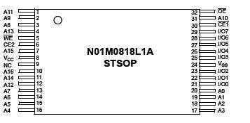
N01M0818L1A: Features: • Single Wide Power Supply Range1.4 to 2.3 Volts - STSOP package• Dual Power Supply - Die Only1.4 to 2.3 Volts - VCC1.4 to 3.6 Volts - VCCQ• Very low standby current200nA...

floor Price/Ceiling Price

Part Number:
N01M0818L1A
Supply Ability:
5000

Price Break

  • Qty
  • 1~5000
  • Unit Price
  • Negotiable
  • Processing time
  • 15 Days
Total Cost: $ 0.00

SeekIC Buyer Protection PLUS - newly updated for 2013!

  • Escrow Protection.
  • Guaranteed refunds.
  • Secure payments.
  • Learn more >>

Month Sales

268 Transactions

Rating

evaluate  (4.8 stars)

Upload time: 2024/4/27

Payment Methods

All payment methods are secure and covered by SeekIC Buyer Protection PLUS.

Notice: When you place an order, your payment is made to SeekIC and not to your seller. SeekIC only pays the seller after confirming you have received your order. We will also never share your payment details with your seller.
Product Details

Description


Features:

• Single Wide Power Supply Range
1.4 to 2.3 Volts - STSOP package
• Dual Power Supply - Die Only
1.4 to 2.3 Volts - VCC
1.4 to 3.6 Volts - VCCQ
• Very low standby current
200nA maximum at 2.0V and 37 deg C
• Very low operating current
1 mA at 2.0V and 1s (Typical)
• Very low Page Mode operating current
0.5mA at 1.0V and 1s (Typical)
• Simple memory control
Dual Chip Enables (CE1 and CE2)
Output Enable (OE) for memory expansion
• Low voltage data retention
Vcc = 1.2V
• Automatic power down to standby mode
• Special Processing to reduce Soft Error Rate (SER)


Pinout

  Connection Diagram


Specifications

Item
Symbol
Rating
Unit
Voltage on any pin relative to VSS
VIN,OUT
0.3 to VCC+0.3
V
Voltage on VCC Supply Relative to VSS
VCC
0.3 to 4.5
V
Power Dissipation
PD
500
mW
Storage Temperature
TSTG
40 to 125
Operating Temperature
TA
-40 to +85
Soldering Temperature and Time
TSOLDER
240,10sec(Lead only)

1. Stresses greater than those listed above may cause permanent damage to the device. This is a stress rating only and functional operation of the device at these or any other conditions above those indicated in the operating section of this specification is not implied. Exposure to absolute maximum rating conditions for extended periods may affect reliability.


Customers Who Bought This Item Also Bought

Margin,quality,low-cost products with low minimum orders. Secure your online payments with SeekIC Buyer Protection.
Prototyping Products
DE1
Circuit Protection
Potentiometers, Variable Resistors
Boxes, Enclosures, Racks
Cable Assemblies
Semiconductor Modules
View more