Features: • Maximum Input Clock Frequency > 3.5 GHz Typical
• Differential CLK Clock Input
• Differential CE Clock Enable Input
• Differential SEL Word Select Input
• 50 Internal Input and Output Termination Resistors
• Differential TC Terminal Count Output
• All Outputs 16 mA CML with 50 Internal Source Termination to VCC
• All SingleEnded Control Pins CMOS and PECL/NECL Compatible
• Counter Programmed Using One of Two Single−Ended Words, Pa[0:7] and Pb[0:7], Stored in REGa and REGb
• REGa and REGb Implemented with Level Triggered Latch
• Compatible with Existing 3.3 V LVEP, EP, and SG Devices
• Ability to Program the Divider without Disturbing Current Settings
• Positive CML Output Operating Range: VCC = 3.0 V to 3.465 V with VEE = 0 V
• Negative CML Output Operating Range: VCC = 0 V with VEE = 3.0 V to 3.465 V
• VBB Reference Voltage Output
• CML Output Level: 400 mV Peak−Peak Output with 50 Receiver Resistor to VCC
• Pb−Free Packages are Available*Pinout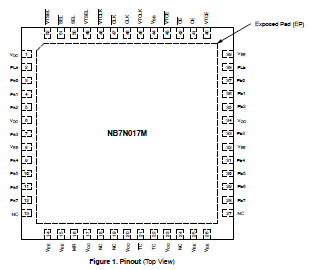 Specifications
|
Symbol |
Parameter |
Condition 1 |
Condition 2 |
Rating |
Units |
|
VCC |
Positive Power Supply |
VEE = 0 V |
|
3.6 |
V |
|
VEE |
Negative Power Supply |
VCC = 0 V |
|
-3.6 |
V |
|
VI |
Positive Input
Negative Input |
VEE = 0 V
VCC = 0 V |
VI VCC
VI VEE |
3.6
-3.6 |
V
V |
|
VINPP |
Differential Input Voltage |CLK − CLK | |
VCC − VEE 2.8 V |
|
2.8V |
V |
|
Iin |
Input Current through RT (50 Resistor) |
Continuous
Surge |
|
25
50 |
mA |
|
Iout |
Output Current |
Continuous
Surge |
|
25
50 |
mA
mA |
|
IBB |
VBB Sink/Source |
|
|
±0.5 |
mA |
|
TA |
Operating Temperature Range |
|
|
−40 to +85 |
|
|
Tstg |
Storage Temperature Range |
|
|
−65 to +150 |
|
|
JA |
Thermal Resistance (Junction−to−Ambient) |
0 lfpm
500 lfpm |
52 QFN
52 QFN |
25 − 32
20 − 27 |
/W
/W |
|
JC |
Thermal Resistance (Junction−to−Case) |
2S2P (Note 8) |
52 QFN |
4-15 |
/W |
|
Tsol |
Wave Solder |
< 2 to 3 seconds |
|
265 |
|
Maximum ratings are those values beyond which device damage can occur. Maximum ratings applied to the device are individual stress limit values (not normal operating conditions) and are not valid simultaneously. If these limits are exceeded, device functional peration is not implied, damage may occur and reliability may be affected.
8. JEDEC standard multilayer board − 2S2P (2 signal, 2 power).
DescriptionThe NB7N017M is a high speed 8bit dual modulus programmable divider/prescaler with 16 mA CML outputs capable of switching at input frequencies greater than 3.5 GHz. The CML output structure contains internal 50 source termination resistor to VCC. The device generates 400 mV output amplitude with 5 0 receiver resistor to VCC. This I/O structure enables easy implementation of the NB7N017M in 50 systems.
The differential inputs contain 50 termination resistors to VT pads and all differential inputs accept RSECL, ECL, LVDS, LVCMOS, LVTTL, and CML.Internally, the NB7N017M uses a > 3.5 GHz 8bit programmable down counter. A select pin, SEL, is used to select between two words, Pa[0:7] and Pb[0:7], that are stored in REGa and REGb respectively. Two parallel load pins, PLa and PLb, are used to load the level triggered programming registers, REGa and REGb, respectively. A differential clock enable, CE, pin is available. The NB7N017M offers a differential output, TC. Terminal count output, TC, goes high for one clock cycle when the counter has reached the all zeros state. To reduce output phase noise, TC is retimed with the rising edge triggered latches.

 NB7N017M Data Sheet


