NBC12430A

Features: • Best−in−Class Output Jitter Performance, ±20 ps Peak−to−Peak• 50 MHz to 800 MHz Programmable Differential PECL Outputs• Fully Integrated Phase−Lock−Loop with Internal Loop Filter• Parallel Interface for Programming Counter and...

product image

NBC12430A Picture
SeekIC No. : 004432737 Detail

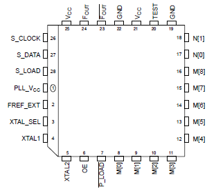
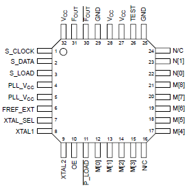
NBC12430A: Features: • Best−in−Class Output Jitter Performance, ±20 ps Peak−to−Peak• 50 MHz to 800 MHz Programmable Differential PECL Outputs• Fully Integrated Phase&#...

floor Price/Ceiling Price

Part Number:
NBC12430A
Supply Ability:
5000

Price Break

  • Qty
  • 1~5000
  • Unit Price
  • Negotiable
  • Processing time
  • 15 Days
Total Cost: $ 0.00

SeekIC Buyer Protection PLUS - newly updated for 2013!

  • Escrow Protection.
  • Guaranteed refunds.
  • Secure payments.
  • Learn more >>

Month Sales

268 Transactions

Rating

evaluate  (4.8 stars)

Upload time: 2024/4/28

Payment Methods

All payment methods are secure and covered by SeekIC Buyer Protection PLUS.

Notice: When you place an order, your payment is made to SeekIC and not to your seller. SeekIC only pays the seller after confirming you have received your order. We will also never share your payment details with your seller.
Product Details

Description


Features:

• Best−in−Class Output Jitter Performance, ±20 ps Peak−to−Peak
• 50 MHz to 800 MHz Programmable Differential PECL Outputs
• Fully Integrated Phase−Lock−Loop with Internal Loop Filter
• Parallel Interface for Programming Counter and Output Dividers uring Powerup
• Minimal Frequency Overshoot
• Serial 3−Wire Programming Interface
• Crystal Oscillator Interface
• Operating Range: VCC = 3.135 V to 5.25 V
• CMOS and TTL Compatible Control Inputs
• Pin and Function Compatible with Motorola MC12430 and PC9230
• 0 to 70 Ambient Operating Temperature (NBC12430)
• −40 to 85 Ambient Operating Temperature (NBC12430A)
• Pb−Free Packages are Available*


Pinout

  Connection Diagram


  Connection Diagram


Specifications

Symbol
Parameter
Condition 1 Condition 2
Rating
Units
VCC
Positive Supply GND = 0 V  
6
V
VI
Input Voltage GND = 0 V VI VCC
6
V
Iout
Output Current Continuous
Surge
 
50
100
mA
mA
TA
Operating Temperature Range  NBC12430
                                                NBC12430A
   
0 to +70
-45 to +85
Tstg
Storage Temperature Range    
-65 to +150
JA
Thermal Resistance (Junction to Ambient) 0 LFPM
500 LFPM
PLCC−28
PLCC−28
63.5
43.5
/W
/W
JC
Thermal Resistance (Junction to Case) Standard Board PLCC−28
22 to 26
/W
JA
Thermal Resistance (Junction to Ambient) 0 LFPM
500 LFPM
LQFP−32
LQFP−32
80
55
/W
/W
JC
Thermal Resistance (Junction to Case) Standard Board LQFP−32
12 to 17
/W
Tsol
Wave Solder                      Pb
                                 Pb−Free
< 3 sec @ 248
< 3 sec @ 260
 
265
265

Maximum ratings are those values beyond which device damage can occur. Maximum ratings applied to the device are individual stress limit values (not normal operating conditions) and are not valid simultaneously. If these limits are exceeded, device  unctional operation is not implied, damage may occur and reliability may be affected.


Description

The NBC12430 and NBC12430A are general purpose, PLL based ynthesized clock sources. The VCO will operate over a frequency  ange of 400 MHz to 800 MHz. The VCO frequency is sent to the −output divider, where NBC12430 and NBC12430A can be configured to provide division ratios f 1, 2, 4, or 8. The VCO and output frequency can be programmed sing the parallel or serial interfaces to the configuration logic. Output requency steps of 250 KHz, 500 KHz, 1.0 MHz, 2.0 MHz can be chieved using a 16 MHz crystal, depending on the output dividers ettings. The PLL loop filter is fully integrated and does not require ny external components.


Customers Who Bought This Item Also Bought

Margin,quality,low-cost products with low minimum orders. Secure your online payments with SeekIC Buyer Protection.
RF and RFID
Line Protection, Backups
Test Equipment
Connectors, Interconnects
Isolators
Optoelectronics
View more