SeekIC No. : 004432771
Detail
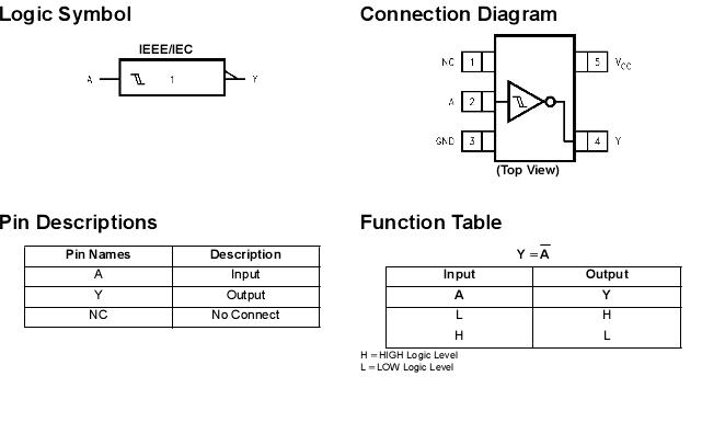
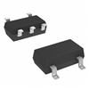
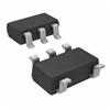
NC7S14: Features: `Space saving SOT23 or SC70 5-lead package` Schmitt input hysteresis: > 1V typ` High speed: tPD 4.5 ns typ` Low quiescent power: ICC < 1 A` Balanced output drive: 2 mA IOL, −2 ...
 NC7S14 Data Sheet
floor Price/Ceiling Price
- Part Number:
- NC7S14
- Supply Ability:
- 5000
Price Break
- Qty
- 1~5000
- Unit Price
- Negotiable
- Processing time
- 15 Days
SeekIC Buyer Protection PLUS - newly updated for 2013!
- Escrow Protection.
- Guaranteed refunds.
- Secure payments.
- Learn more >>
Month Sales
268 Transactions
Payment Methods
All payment methods are secure and covered by SeekIC Buyer Protection PLUS.
Notice: When you place an order, your payment is made to SeekIC and not to your seller. SeekIC only pays the seller after confirming you have received your order. We will also never share your payment details with your seller.