NLSF595

Features: • Parallel Outputs are Open Drain Capable of Sinking > 12 mA Output Withstands up to +7.0 Regardless of VCC• Standard Serial (SPI) Interface, Data, Clock, Enable (Low)• All Inputs CMOS Level Compatible• Frees up I/O around a Microcontroller• Only One Pin ...

product image

NLSF595 Picture
SeekIC No. : 004434809 Detail

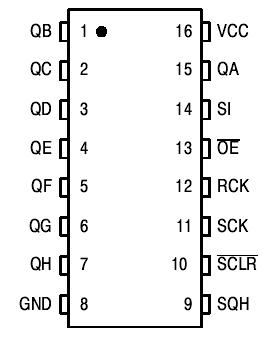
NLSF595: Features: • Parallel Outputs are Open Drain Capable of Sinking > 12 mA Output Withstands up to +7.0 Regardless of VCC• Standard Serial (SPI) Interface, Data, Clock, Enable (Low)•...

floor Price/Ceiling Price

Part Number:
NLSF595
Supply Ability:
5000

Price Break

  • Qty
  • 1~5000
  • Unit Price
  • Negotiable
  • Processing time
  • 15 Days
Total Cost: $ 0.00

SeekIC Buyer Protection PLUS - newly updated for 2013!

  • Escrow Protection.
  • Guaranteed refunds.
  • Secure payments.
  • Learn more >>

Month Sales

268 Transactions

Rating

evaluate  (4.8 stars)

Upload time: 2024/4/26

Payment Methods

All payment methods are secure and covered by SeekIC Buyer Protection PLUS.

Notice: When you place an order, your payment is made to SeekIC and not to your seller. SeekIC only pays the seller after confirming you have received your order. We will also never share your payment details with your seller.
Product Details

Description


Features:

• Parallel Outputs are Open Drain Capable of Sinking > 12 mA Output Withstands up to +7.0 Regardless of VCC
• Standard Serial (SPI) Interface, Data, Clock, Enable (Low)
• All Inputs CMOS Level Compatible
• Frees up I/O around a Microcontroller
• Only One Pin Dedicated to this Device (Latch Enable)
• Output Enable may be Permanently Pulled Low
• High Speed Clocking, Fmax > 25 MHz (Shift Clock)
• Eight Bits Parallel Output
• Double Buffered Outputs, so Register may Fill without Affecting Output
• STD CMOS Serial Output, may be used to Cascade more than One Device
• Each Part Controls Two Tri−Color LEDs
• Two Devices can Control 5 Tri−Color LEDs
• Low Leakage: ICC = 2.0 A (Max) at TA = 25°C
• Latchup Performance Exceeds 100 mA
• QFN−16/TSSOP−16 Packages
• ESD Performance: Human Body Model; > 2000 V, Machine Model; > 200 V
• Functionally Similar to the Popular 74VHC595
• Pb−Free Packages are Available


Pinout

  Connection Diagram


Specifications

Symbol Parameter Value Unit
VCC Positive DC Supply Voltage -0.5 to +7.0 V
VIN DC Input Voltage -0.5 to +7.0 V
VOUT DC Output Voltage -0.5 to VCC +7.0 V
IIk Input Diode Current -20 mA
IOK Output Diode Current ±50 mA
IOUT DC Output Current,per Pin ±50 mA
ICC DC Supply Current,VCC and GND Pins ±75 mA
PD Power Dissipation in Still Air 450 mW
TSTG Storage Temperature Range -65 to +150
ILATCHUP Latchup Performance Above VCC and Below GND at 125°C (Note ±300 mA
JA Thermal Resistance, Junction−to−Ambient 128 /W

Maximum ratings are those values beyond which device damage can occur. Maximum ratings applied to the device are individual stress limit values (not normal operating conditions) and are not valid simultaneously. If these limits are exceeded, device functional operation is not implied, damage may occur and reliability may be affected.
1. Tested to EIA/JESD78


Description

The NLSF595 is advanced CMOS shift register with open drain outputs fabricated with 0.6 m silicon gate CMOS technology. This device is used in conjunction with a microcontroller, with only onededicated line. All pins of NLSF595 have Overvoltage Protection that allows voltages above VCC up to 7.0 V to be present on the pins without damage or disruption of operation of the part, regardless of the operating voltage. This device may be used between 2.0 and 5.5 volts, the output driver level may be independent of supply voltage: 0−7.0 volts.


Customers Who Bought This Item Also Bought

Margin,quality,low-cost products with low minimum orders. Secure your online payments with SeekIC Buyer Protection.
LED Products
Power Supplies - Board Mount
Motors, Solenoids, Driver Boards/Modules
Isolators
Cables, Wires
View more