NTHD2102P

Features: • Offers an Ultra Low RDS(on) Solution in the ChipFET Package• Miniature ChipFET Package 40% Smaller Footprint than TSOP−6 making it an Ideal Device for Applications where Board Space is at a Premium• Low Profile (<1.1 mm) Allows it to Fit Easily into Extremely...

product image

NTHD2102P Picture
SeekIC No. : 004436663 Detail

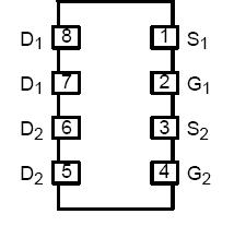
NTHD2102P: Features: • Offers an Ultra Low RDS(on) Solution in the ChipFET Package• Miniature ChipFET Package 40% Smaller Footprint than TSOP−6 making it an Ideal Device for Applications wher...

floor Price/Ceiling Price

Part Number:
NTHD2102P
Supply Ability:
5000

Price Break

  • Qty
  • 1~5000
  • Unit Price
  • Negotiable
  • Processing time
  • 15 Days
Total Cost: $ 0.00

SeekIC Buyer Protection PLUS - newly updated for 2013!

  • Escrow Protection.
  • Guaranteed refunds.
  • Secure payments.
  • Learn more >>

Month Sales

268 Transactions

Rating

evaluate  (4.8 stars)

Upload time: 2024/4/26

Payment Methods

All payment methods are secure and covered by SeekIC Buyer Protection PLUS.

Notice: When you place an order, your payment is made to SeekIC and not to your seller. SeekIC only pays the seller after confirming you have received your order. We will also never share your payment details with your seller.
Product Details

Description


Features:

• Offers an Ultra Low RDS(on) Solution in the ChipFET Package
• Miniature ChipFET Package 40% Smaller Footprint than TSOP−6
  making it an Ideal Device for Applications where Board Space is at a Premium
• Low Profile (<1.1 mm) Allows it to Fit Easily into Extremely Thin
  Environments such as Portable Electronics
• Designed to Provide Low RDS(on) at Gate Voltage as Low as 1.8 V, the
  Operating Voltage used in many Logic ICs in Portable Electronics
• Simplifies Circuit Design since Additional Boost Circuits for Gate
  Voltages are not Required
• Operated at Standard Logic Level Gate Drive, Facilitating Future
  Migration to Lower Levels using the same Basic Topology
• Pb−Free Package is Available


Application

• Optimized for Battery and Load Management Applications in
  Portable Equipment such as MP3 Players, Cell Phones, Digital
  Cameras, Personal Digital Assistant and other Portable Applications
• Charge Control in Battery Chargers
• Buck and Boost Converters


Pinout

  Connection Diagram


Specifications

Rating Symbol Value Unit
Drain−to−Source Voltage VDSS −8.0 V
Gate−to−Source Voltage − Continuous VGS ±8.0 V
Drain Current − Continuous
− 5 seconds
lD
lD
−3.4
−4.6
A
Total Power Dissipation
Continuous @ TA = 25°C
(5 sec) @ TA = 25°C
Continuous @ 85°C
(5 sec) @ 85°C
PD 1.1
2.1
0.6
1.1
W
Operating Junction and Storage Temperature
Range
TJ, Tstg −55 to
+150
°C
Continuous Source Current
(Diode Conduction)
ls −1.1 A
Thermal Resistance (Note 1)
Junction−to−Ambient, 5 sec
Junction−to−Ambient, Continuous
RJA
RJA
60
113
°C/W
Maximum Lead Temperature for Soldering
Purposes, 1/8, from case for 10 seconds
TL

260

°C
Maximum ratings are those values beyond which device damage can occur.
Maximum ratings applied to the device are individual stress limit values (not
normal operating conditions) and are not valid simultaneously. If these limits are
exceeded, device functional operation is not implied, damage may occur and
reliability may be affected.
1. Surface Mounted on FR4 Board using 1 in sq pad size (Cu area = 1.27 in sq
[1 oz] including traces).


Customers Who Bought This Item Also Bought

Margin,quality,low-cost products with low minimum orders. Secure your online payments with SeekIC Buyer Protection.
Soldering, Desoldering, Rework Products
Industrial Controls, Meters
Cable Assemblies
Programmers, Development Systems
Sensors, Transducers
Tapes, Adhesives
803
View more