Pinout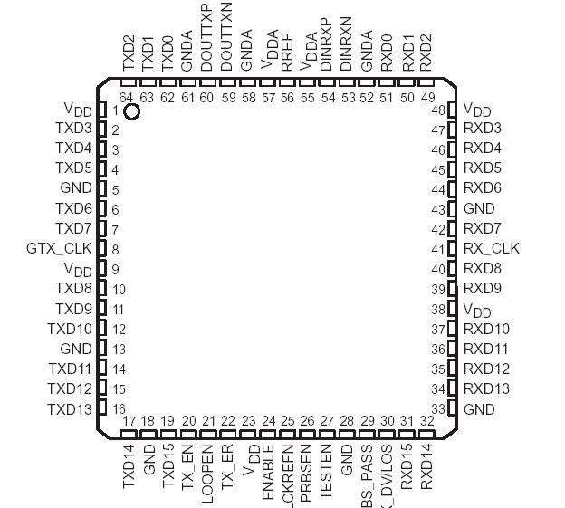
SpecificationsSupply voltage, VDD (see Note 1) . . . . . . . . . . . . . . . . . . . . . . . . . . . . . . . . . . . .0.3 to 3 V
Voltage range at TXD, ENABLE, GTX_CLK, TX_EN, TX_ER, LOOPEN, PRBS_PASS .0.3 to 4 V
Voltage range at any other terminal except above . . . . . . . . . . . . . . . . .0.3 to VCC+0.3 V
Package power dissipation, PD . . . . . . . . . . . . . . . . . . . . . . . . .See Dissipation Rating Table
Storage temperature, Tstg . . . . . . . . . . . . . . . . . . . . . . . . . . . . . . . . . . . .65°C to 150°C
Electrostatic discharge . . . . . . . . . . . . . . . . . . . . . . . . . . . . . . . . . . . . .HBM:3 KV, CDM:1.5 KV
Characterized free-air operating temperature range, TA . . . . . . . . . .. . . . . .40°C to 85°C
Lead temperature 1,6 mm (1/16 inch) from case for 10 seconds . . . . . . . . . . . . . . . .260°C
NOTE 1: All voltage values, except differential I/O bus voltages, are with respect to network ground.DescriptionThe PCI6060 is a serial PCI transceiver, intended for use in the PCI6050 symmetric serialized PCI-PCI bridge. The PCI6050 bridge provides a high-performance solution for connecting two PCI buses via an ultrahigh-speed bidirectional cable medium. The PCI6060 supports an effective serial interface speed of 1.6 Gbps to 2.5 Gbps providing up to 2.0 Gbps of data bandwidth. The primary application of this chip is to provide very high-speed I/O data channels for point-to-point baseband data transmission over controlled impedance media of approximately 50 W. The transmission media can be printed-circuit board, copper cables, or fiber-optic cable. The maximum rate and distance of data transfer is dependent upon the attenuation characteristics of the media and the noise coupling to the environment.
This device can also be used to replace parallel data transmission architectures by providing a reduction in the number of traces, connector terminals, and transmit/receive terminals. Parallel data loaded into the transmitter is delivered to the receiver over a serial channel, which can be a coaxial copper cable, a controlled impedance backplane, or an optical link. It is then reconstructed into its original parallel format. It offers significant power and cost savings over current solutions, as well as scalability for higher data rate in the future.
The PCI6060 performs data conversion parallel-to-serial and serial-to-parallel. The clock extraction functions as a physical layer interface device. The serial transceiver interface operates at a maximum speed of 2.5 Gbps. The transmitter latches 16-bit parallel data at a rate based on the supplied reference clock (GTX_CLK). The 16-bit parallel data is internally encoded into 20 bits using an 8-bit/10-bit (8B/10B) encoding format. The resulting 20-bit word is then transmitted differentially at 20 times the reference clock (GTX_CLK) rate. The receiver section performs the serial-to-parallel conversion on the input data, synchronizing the resulting 20-bit wide parallel data to the extracted reference clock (RX_CLK). It then decodes the 20 bit wide data using 8-bit/10-bit decoding format resulting in 16 bits of parallel data at the receive data terminals (RXD0-15). The outcome is an effective data payload of 1.28 Gbps to 2.0 Gbps (16 bits data x the GTX_CLK frequency).
The PCI6060 is housed in a high performance, thermally enhanced, 64-pin PQFP PowerPADE package. Use of the PowerPADE package does not require any special considerations except to note that the PowerPADE, which is an exposed die pad on the bottom of the device, is a metallic thermal and electrical conductor. It is recommended that the PCI6060 PowerPADE be soldered to the thermal land on the board. All ac performance specifications in this data sheet are measured with the PowerPADE soldered to the test board.
The PCI6060 provides an internal loopback capability for self-test purposes. Serial data from the serializer is passed directly to the deserializer, allowing the protocol device a functional self-check of the physical interface. The PCI6060 is designed to be hot plug capable. An on-chip power-on reset circuit holds the RX_CLK low and goes to high impedance to the parallel side output signal terminals during power up as well as goes to DOUTTXP and DOUTTXN.
The PCI6060 has a loss of signal detection circuit for conditions where the incoming signal no longer has a sufficient voltage amplitude to keep the clock recovery circuit in lock.
To prevent a data bit error from causing a valid data packet from being interpreted as a comma and thus causing the erroneous word alignment by the comma detection circuit, the comma word alignment circuit is turned off after the link is properly established in PCI6060.
The PCI6060 allows users to implement redundant ports by connecting receive data bus terminals from two PCI6060 devices together. Asserting the LCKREFN to go to a low state will cause the receive data bus terminals, RXD[0:15], RX_CLK and RX_ER, RX_DV/LOS to go to a high impedance state. This places the device in a transmit only mode since the receiver is not tracking the data.
The PCI6060 uses a 2.5-V supply. The I/O section is 3 V compatible. With the 2.5-V supply the chipset is very power-efficient, consuming less than 325 mW typically. The PCI6060 is characterized for operation from 40°C to 85°C.

 PCI6060 Data Sheet