Features: • PI4ULS3V08M is designed for low voltage operation:1.2V to 3.6V
• Universal bidirectional level shifting with automatic direction control
• Fast bus speeds up to 160 Mbps
• IOFF supports partial Power-Down mode operation
• Drive Capability 12mA
• Independent translation of each bit
• Each supply rail is configurable over supply range
• ESD Protection exceeds JESD22 2000V Human Body Model (A114-B) 200V Machine Model (A115-A)
• Latch-up performance exceeds 100mA per JESD 78
• Industrial operation at 40°C to +85°C
• Packaging (Pb-free & Green): 32-contact TQFN (ZL)Application• Voltage Translation
• Bus Relay
• Mobile DevicesPinout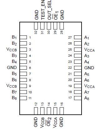 Specifications
Supply voltage range: VCCA........................................................................................................ 0.5V to 4.6V
VCCB ........................................................................................................................................... 0.5V to 4.6V
Input voltage range, VI(1) Control Inputs.................................................................................. 0.5V to 4.6V
Voltage Range applied to any I/O pins in the high-impedance or Power-Off state, VIO (1) :
A Port ....................................................................................................................................... 0.5V to 4.6V
B Port.......................................................................................................................................... 0.5V to 4.6V
Voltage Range applied to any I/O pins in the High or Low state VIO (1, 2): A Port .........0.5V to VCCA +0.5V
B Port.............................................................................................................................. 0.5V to VCCB +0.5V
Input clamp current, IIK (VI <0).............................................................................................................. 50mA
Output clamp current, IOK (VO <0).......................................................................................................... 50mA
Continuous output current, IO ................................................................................................................ ±20mA
Continuous current through VCCA, VCCB or GND .................................................................................... ±100mA
Storage temperature range, TSTG ........................................................................................... 65°C to 150°C
Note:
1. The input negative voltage and output voltage ratings may be exceeded if the input and output current ratings are observed.
2. This value is limited to 3.6V maximum.
3. Stresses greater than those listed under MAXIMUM RATINGS may cause permanent damage to the device. This is a stress rating only and functional operation of the device at these or any other conditions above those indicated in the operational sections of this specification is not implied. Exposure to absolute maximum rating conditions for extended periods may affect reliability.
DescriptionPI4ULS3V08M, is a 8-bit (octal) non-inverting bus transceiver with two separate supply rails: A port (VCCA) and B port (VCCB) are set to operate at 1.2V to 3.6V. This arrangement permits universal bidirectional translation of differential signal levels over the voltage ranges.
The PI4ULS3V08M is designed for asynchronous communication between data buses. Data is transmitted from the A bus to the B bus, or vice versa, without direction control. All AX, and BX are tri-stated when data is coming from both directions at the same time. The output-enable (OE) input is used to disable outputs so buses are isolated.
The control pins of PI4ULS3V08M , OEx, TEST_EN and OUT_SEL are supplied by VCCB.
The PI4ULS3V08M is fully specified for partial-power-down applications using IOFF. The IOFF circuitry disables the outputs, preventing damaging current backflow through the device when it is powered down.To ensure the high impedance state during power-up or power-down, the output-enable (OEx) input should be tied to VCC through a pullup resistor: the minimum value of the resistor is determined by the current-sinking capability of the driver.

 PI4ULS3V08M Data Sheet


