PIC32MX

Features: Special Microcontroller Features:· Operating Voltage Range of 2.5V to 3.6V· 32-512K Flash and 8-32K Data Memory· Additional 12 KB of Boot Flash Memory· Pin-Compatible with most PIC24/dsPIC® Devices· Multiple Power Management Modes· Multiple Interrupt Vectors with Individually Program...

product image

PIC32MX Picture
SeekIC No. : 004462598 Detail

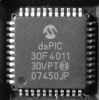
PIC32MX: Features: Special Microcontroller Features:· Operating Voltage Range of 2.5V to 3.6V· 32-512K Flash and 8-32K Data Memory· Additional 12 KB of Boot Flash Memory· Pin-Compatible with most PIC24/dsPIC...

floor Price/Ceiling Price

Part Number:
PIC32MX
Supply Ability:
5000

Price Break

  • Qty
  • 1~5000
  • Unit Price
  • Negotiable
  • Processing time
  • 15 Days
Total Cost: $ 0.00

SeekIC Buyer Protection PLUS - newly updated for 2013!

  • Escrow Protection.
  • Guaranteed refunds.
  • Secure payments.
  • Learn more >>

Month Sales

268 Transactions

Rating

evaluate  (4.8 stars)

Upload time: 2024/3/27

Payment Methods

All payment methods are secure and covered by SeekIC Buyer Protection PLUS.

Notice: When you place an order, your payment is made to SeekIC and not to your seller. SeekIC only pays the seller after confirming you have received your order. We will also never share your payment details with your seller.
Product Details

Description


Features:

Special Microcontroller Features:
· Operating Voltage Range of 2.5V to 3.6V
· 32-512K Flash and 8-32K Data Memory
· Additional 12 KB of Boot Flash Memory
· Pin-Compatible with most PIC24/dsPIC® Devices
· Multiple Power Management Modes
· Multiple Interrupt Vectors with Individually Programmable Priority
· Fail-Safe Clock Monitor Mode
· Configurable Watchdog Timer with On-Chip, Low-Power RC Oscillator for Reliable Operation
· Two Programming and Debugging Interfaces:
- 2-wire interface with unintrusive access and real-time data exchange with application
- 4-wire MIPS standard enhanced JTAG interface
· Unintrusive Hardware-Based Instruction Trace
· IEEE Std 1149.2 Compatible (JTAG) Boundary Scan

Analog Features:
· Up to 16-Channel 10-Bit Analog-to-Digital Converter:
- 400 ksps conversion rate
- Conversion available during Sleep, Idle
· Two Analog Comparators

Peripheral Features:
· Atomic SET, CLEAR and INVERT Operation on Select Peripheral Registers
· Up to 4-Channel Hardware DMA Controller with Automatic Data Size Detection
·Two I2CTM Modules
· Two UART Modules with:
- RS-232, RS-485 and LIN 1.2 support
- IrDA® with on-chip hardware encoder and decoder
· Parallel Master and Slave Port (PMP/PSP) with 8-Bit and 16-Bit Data and Up to 16 Address Lines
· Hardware Real-Time Clock/Calendar (RTCC)
· Five 16-Bit Timers/Counters (two 16-bit pairs combine to create two 32-bit timers)
· Five Capture Inputs
· Five Compare/PWM Outputs
· Five External Interrupt pins
· 5V Tolerant Input Pins
· 8 mA Sink/Source on Select I/O Pins
· Configurable Open-Drain Output on Digital I/O Pins


Specifications

Ambient temperature under bias.........................................................................................................-40°C to +85°C
Storage temperature ...................................................................................................................... -65°C to +150°C
Voltage on VDD with respect to VSS ..................................................................................................... -0.3V to +4.0V
Voltage on any combined analog and digital pin and MCLR, with respect to VSS ........................ -0.3V to (VDD + 0.3V)
Voltage on any digital only pin with respect to VSS ............................................................................... -0.3V to +5.5V
Voltage on VDDCORE with respect to VSS ................................................................................................ -0.3V to 2.0V
Maximum current out of VSS pin .........................................................................................................................TBD mA
Maximum current into VDD pin (Note 2)...............................................................................................................TBD mA
Maximum output current sunk by any I/O pin (Note 3) ......................................................................................TBD mA
Maximum output current sourced by any I/O pin (Note 3) .................................................................................TBD mA
Maximum current sunk by all ports .....................................................................................................................TBD mA
Maximum current sourced by all ports (Note 2)...................................................................................................TBD mA
Legend: TBD = To Be Determined
Note 1: Stresses above those listed under 'Absolute Maximum Ratings' may cause permanent damage to the device. This is a stress rating only and functional operation of the device at those or any other conditions above those indicated in the operation listings of this specification is not implied. Exposure to maximum rating conditions for extended periods may affect device reliability.
2: Maximum allowable current is a function of device maximum power dissipation (see Table 29-2).
3: Exceptions are CLKOUT, which is able to sink/source 25 mA, and the VREF+, VREF-, SCLx, SDAx, PGCx and PGDx pins, which are able to sink/source 12 mA.


Customers Who Bought This Item Also Bought

Margin,quality,low-cost products with low minimum orders. Secure your online payments with SeekIC Buyer Protection.
Industrial Controls, Meters
Undefined Category
Programmers, Development Systems
Test Equipment
Cables, Wires
View more