PMB 2362

Features: Worldclass B6HF technology, fT = 25GHz Lowest external component count Extreme small outline P-TSSOP-10-2 package with heat sink for grounding Both LNAs with prematched input, only 2 external matching components required GSM900 LNA output matched to 50 Ohm Both LNAs with switchable gain,...

product image

PMB 2362 Picture
SeekIC No. : 004463936 Detail

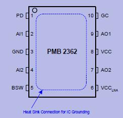
PMB 2362: Features: Worldclass B6HF technology, fT = 25GHz Lowest external component count Extreme small outline P-TSSOP-10-2 package with heat sink for grounding Both LNAs with prematched input, only 2 exter...

floor Price/Ceiling Price

Part Number:
PMB 2362
Supply Ability:
5000

Price Break

  • Qty
  • 1~5000
  • Unit Price
  • Negotiable
  • Processing time
  • 15 Days
Total Cost: $ 0.00

SeekIC Buyer Protection PLUS - newly updated for 2013!

  • Escrow Protection.
  • Guaranteed refunds.
  • Secure payments.
  • Learn more >>

Month Sales

268 Transactions

Rating

evaluate  (4.8 stars)

Upload time: 2024/4/28

Payment Methods

All payment methods are secure and covered by SeekIC Buyer Protection PLUS.

Notice: When you place an order, your payment is made to SeekIC and not to your seller. SeekIC only pays the seller after confirming you have received your order. We will also never share your payment details with your seller.
Product Details

Description


Features:

 Worldclass B6HF technology, fT = 25GHz
Lowest external component count
Extreme small outline P-TSSOP-10-2 package with heat sink for grounding
Both LNAs with prematched input, only 2 external matching components required
GSM900 LNA output matched to 50 Ohm
Both LNAs with switchable gain, 20dB gain step
LNA1: 17dB gain, 1.5dB noise figure @ 0.95GHz
LNA2: 19dB gain, 2.0dB noise figure @ 1.85GHz
Supply voltage range from 2.7V to 3.6V
Power down function
Temperature range -40° to 85°C


Application

 Dual band wireless frontends GSM900/1800
 Excellent combination with Infineon GSM single chip SMARTiPMB 6250


Pinout

  Connection Diagram


Specifications

Parameter Symbol Limit Values Unit Remarks
min max
Supply Voltage VVCC -0.3 5.0 V  
Input Voltage VPD -0.3 VS +0.3,
5.0max.
V  
Input Voltage VBSW -0.3 VS +0.3,
5.0max.
V  
Input Voltage VGC -0.3 VS +0.3,
5.0max.
V VPD>0.5V
Input Voltage VGC -0.3 3.8 V VPD=0V
Input Voltage
(AC Peak, Freq.>1MHz)
VAI1/2 VS -5.5,
-2.0min.
  V VPD=0V
IAI1/2<nA
Open Collector Output Voltage VAO2/VCCLNA VS -5.5,
-0.3min
VS +2.0,
5.0max.
V  
Input Current IAI1/2   6.0 mA DC and AC
Junction Temperature Tj   125 °C  
Storage Temperature TS -40 125 °C  
Thermal Resistance RthJA   100 K/W Junction to
Ambient
Thermal Resistance RthJL   12 K/W *Junction to
Lead
ESD integrity VESD -1000 +1000 V **
* Heat Sink Temperature Fixed At 25 ° Celsius
** According to MIL STD 883D, method 3015.7 and ESD Assn.
Standard S5.1 - 1993.


Description

The PMB2362 is a dual band LNA circuit with excellent performance and minimum component count for GSM900 and GSM1800.


Customers Who Bought This Item Also Bought

Margin,quality,low-cost products with low minimum orders. Secure your online payments with SeekIC Buyer Protection.
Motors, Solenoids, Driver Boards/Modules
Soldering, Desoldering, Rework Products
Resistors
Semiconductor Modules
Batteries, Chargers, Holders
View more