QS53805

Features: - 10 output, low skew clock signal buffer- Pinout and function compatible with QS5805T- JEDEC compatible LVTTL inputs and outputs- Input hysteresis for better noise margin- Monitor output- Guaranteed low skew:· 0.7ns output skew· 1.1ns pulse skew· 1ns part-to-part skew- Clock inputs are ...

product image

QS53805 Picture
SeekIC No. : 004468511 Detail

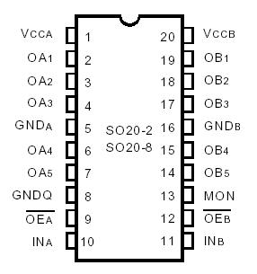
QS53805: Features: - 10 output, low skew clock signal buffer- Pinout and function compatible with QS5805T- JEDEC compatible LVTTL inputs and outputs- Input hysteresis for better noise margin- Monitor output-...

floor Price/Ceiling Price

Part Number:
QS53805
Supply Ability:
5000

Price Break

  • Qty
  • 1~5000
  • Unit Price
  • Negotiable
  • Processing time
  • 15 Days
Total Cost: $ 0.00

SeekIC Buyer Protection PLUS - newly updated for 2013!

  • Escrow Protection.
  • Guaranteed refunds.
  • Secure payments.
  • Learn more >>

Month Sales

268 Transactions

Rating

evaluate  (4.8 stars)

Upload time: 2024/5/15

Payment Methods

All payment methods are secure and covered by SeekIC Buyer Protection PLUS.

Notice: When you place an order, your payment is made to SeekIC and not to your seller. SeekIC only pays the seller after confirming you have received your order. We will also never share your payment details with your seller.
Product Details

Description


Features:

-  10 output, low skew clock signal buffer
-  Pinout and function compatible with QS5805T
-  JEDEC compatible LVTTL inputs and outputs
-  Input hysteresis for better noise margin
-  Monitor output
-  Guaranteed low skew:
·  0.7ns output skew
·  1.1ns pulse skew
·  1ns part-to-part skew
-  Clock inputs are 5V tolerant
-  Std. and A speed grades
-  Available in QSOP and SOIC packages


Pinout

  Connection Diagram


Specifications

Rating
Symbol
Max
unit
Supply Voltage Range
V CC1, VCC2
0.5 to +4.6
V
Input Voltage Range
VI (2)
0.5 to +5.5
V
Voltage range applied to any
output in the high or low state
VO(2)
0.5 to VDD + 0.5
V
Input clamp current
IIK (VI < 0)
50
mA
Terminal Voltage with Respect
to GND (inputs VIH 2.5, VIL 2.5)
IOK
(VO < 0 or VO > VDD)
-50
mA
Continuous Output Current
IRES
±100
mA
Continuous Current
VDD or GND
65 to +150
mA
Junction Temperature
TSTG
150
°C


NOTES:
1. Stresses greater than those listed under ABSOLUTE MAXIMUM RATINGS may cause permanent damage to the device. This isstress rating only and functional operation of the device at these or any other conditions above those indicated in the operational sections of this specification is not implied. Exposure to absolute maximum rating conditions for extended periods may affect reliability.
2. Vcc Terminals.
3. All terminals except Vcc.


Description

The QS53805 clock buffer/driver circuits can be used for clock buffering schemes where low skew is a key parameter. This device offers two banks of 5 non-inverting outputs. The QS53805 device provides low propagation delay buffering with on-chip skew of 0.7ns for same-transition, same-bank signals. This clock buffer product is designed for use in high performance workstations, embedded and personal computing systems using 3V to 3.6V supply voltages. Several can be used in parallel or scattered throughout a system for guaranteed low skew, system-wide clock distribution networks.

The QS53805 can accept 5V input and control signals. The QS53805 is characterized for operation at -40°C to +85°C.


Customers Who Bought This Item Also Bought

Margin,quality,low-cost products with low minimum orders. Secure your online payments with SeekIC Buyer Protection.
Undefined Category
Transformers
Tapes, Adhesives
803
Programmers, Development Systems
Cables, Wires
View more