Features: • Output Current..................... 100mA (MAX. at VIN=5.0V, CIN=CP=COUT=4.7µF, Set Output Voltage=-3.0V)
• Output Voltage Accuracy...... ±3.0% (VIN=5.0V, CIN=CP=COUT=4.7µF, Set Output Voltage=-3.0V, IOUT=0mA/10mA) ±9.0% (VIN=5.0V, CIN=CP=COUT=4.7µF, Set Output Voltage=-3.0V, IOUT=50mA)
• Output Voltage...................... Stepwise setting with a step of 0.1V in the range from -2.0V to -4.0V is possible.
• Range of Input Voltage ......... VOUTV to +5.5V (Set Output Voltage=-4.0V to -2.8V) +2.7V to +5.5V (Set Output Voltage=-2.7V to -2.0V)
• Oscillator Frequency ............ TYP. 280kHz
• Chip Enable Function (Active at “L”)
• Package ................................. TSSOP8
Application• Power source for Disk Drives.
• Power source for hand-held communication equipment and battery-powered equipment.
• Power source for PC peripherals and ADD-ON cards.
• Power source for portable audio-visual appliances such as cameras.
• Local power source for small electrical appliances.Pinout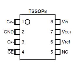 Specifications
| Symbol |
Item |
Rating |
Unit |
| VIN |
VIN Supply Voltage |
-0.3 to 7.5 |
V |
| VCE |
CE Pin Input Voltage |
-0.3 to VIN+0.3 |
V |
| VP+ |
CP+ Pin Input Voltage |
-0.3 to VIN+0.3 |
V |
| Vref |
Vref Pin Voltage |
-0.3 to VIN+0.3 |
V |
| VP- |
CP- Pin Input Voltage |
VIN-12 to +0.3 |
V |
| VOUT |
VOUT Pin Voltage |
VIN-12 to +0.3 |
V |
| IOUT |
Output Current |
200 |
mA |
| PD |
Power Dissipation*NOTE1 |
490 |
mW |
| Topt |
Operating Temperature Range |
-40 to +85 |
°C |
| Tstg |
Storage Temperature Range |
-55 to +125 |
°C |
DescriptionThe R1250V××1A Series are Negative Output Charge Pump Regulator ICs, which can be developed as local power suppliers for portable appliances and small electric appliances used with batteries, with low supply current by CMOS process.
Each of these ICs consists of an oscillator, a control circuit, a reference voltage unit, an error amplifier, and an output driver circuit. The R1250V××1A can easily supply negative voltage, or regulated setting output voltage in the range from -2V to -4V from positive input voltage.
The chip enable function works to shut down the internal circuit and reduces supply current at the stand-by mode, therefore the R1250V××1A is very suitable for the application such as portable systems that require low supply current.
Since the package for R1250V××1A is TSSOP8 package (TSOP8 in EIAJ standard), high density mounting of the ICs on board is possible.

 R1250V××1A Data Sheet


