Features: • Direct display of RAM data through the display data RAM.
RAM bit data: "1" Display on
"0" Display off
(during normal display)
• RAM capacity
65 ´ 132 = 8580 bits
• Display driver circuits
S1D15605*****:65 common output and 132 segment outputs
S1D15606*****:49 common output and 132 segment outputs
S1D15607*****:33 common outputs and 132 segment outputs
S1D15608*****:55 common outputs and 132 segment outputs
S1D15609*****:53 common outputs and 132 segment outputs
• High-speed 8-bit MPU interface (The chip can be connected directly to the both the 80x86 series MPUs and the 68000 series MPUs) /Serial interfaces are supported.
• Abundant command functions
Display data Read/Write, display ON/OFF, Normal/ Reverse display mode, page address set, display start line set, column address set, status read, display all points ON/OFF, LCD bias set, electronic volume, read/modify/write, segment driver direction select, power saver, static indicator, common output status select, V5 voltage regulation internal resistor ratio set.
• Static drive circuit equipped internally for indicators.
(1 system, with variable flashing speed.)
• Low-power liquid crystal display power supply circuit equipped internally.
Booster circuit (with Boost ratios of Double/Triple/ Quad, where the step-up voltage reference power supply can be input externally)
High-accuracy voltage adjustment circuit (Thermal gradient 0.05%/°C or 0.2%/°C or external input) V5 voltage regulator resistors equipped internally, V1 to V4 voltage divider resistors equipped internally, electronic volume function equipped internally, voltage follower.
• CR oscillator circuit equipped internally (external clock can also be input)
• Extremely low power consumption
Operating power when the built-in power supply is used (an example)
S1D15605D00B* 81 mA (VDD VSS = VDD VSS2= /S1D15605D11B* 3.0 V, Quad voltage, V5 VDD = 11.0 V)
S1D15606D00B* 43 mA (VDD VSS = VDD VSS2 = /S1D15606D11B* 3.0 V, Triple voltage, V5 VDD = 8.0 V)
S1D15607D00B* 29 mA (VDD VSS = VDD VSS2 = /S1D15607D11B* 3.0 V, Triple voltage, V5 VDD = 8.0 V)
S1D15608D00B*/S1D15608D11B*
/S1D15609D00B*/S1D15609D11B*
46mA (VDD VSS = VDD VSS2 = 3.0 V, Triple voltage, V5 VDD = 8.0 V)
Conditions: When all displays are in white and the normal mode is selected (see page 60 *12 for details of the conditions).
• Power supply
Operable on the low 1.8 voltage
Logic power supply VDD VSS = 1.8 V to 5.5 V
Boost reference voltage: VDD VSS2 = 1.8 V to 6.0 V
Liquid crystal drive power supply: V5 VDD = 4.5 V to 16.0 V
• Wide range of operating temperatures: 40 to 85°C
• CMOS process
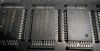
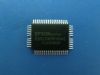
• Shipping forms include bare chip and TCP.
• These chips not designed for resistance to light or resistance to radiation.
Pinout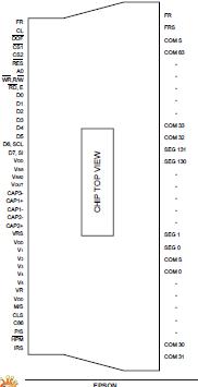 Specifications
| Parameter |
Symbol |
Conditions |
Unit |
| Power Supply Voltage |
VDD |
0.3 to +7.0 |
V |
Power supply voltage (2)
(VDD standard) |
With Triple step-up
With Quad step-up |
VSS2 |
7.0 to +0.3
6.0 to +0.3
4.5 to +0.3 |
V |
| Power supply voltage (3) (VDD standard) |
V5, VOUT |
18.0 to +0.3 |
V |
| Power supply voltage (4) (VDD standard) |
V1, V2, V3, V4 |
V5 to +0.3 |
V |
| Input voltage |
VIN |
0.3 to VDD + 0.3 |
V |
| Output voltage |
VO |
0.3 to VDD + 0.3 |
V |
| Operating temperature |
TOPR |
40 to +85 |
°C |
| Storage temperature |
TCP
Bare chip |
TSTR |
55 to +100
55 to +125 |
°C |
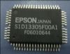
DescriptionThe S1D15605 Series is a series of single-chip dot matrix liquid crystal display drivers that can be connected directly to a microprocessor bus. 8-bit parallel or serial display data sent from the microprocessor is stored in the internal display data RAM and the chip generates a liquid crystal drive signal independent of the microprocessor. Because the chips in the S1D15605***** contain 65 ´ 132 bits of display data RAM and there is a 1-to-1 correspondence between the liquid crystal panel pixels and the internal RAM bits, these chips enable displays with a high degree of freedom.
The S1D15606***** chips contain 49 common output circuits and 132 segment output circuits, so that a single chip can drive a 49 ´ 132 dot display (capable of displaying 8 columns ´ 4 rows of a 16 ´ 16 dot kanji font). The S1D15607***** chips contain 33 common output circuits and 132 segment output circuits, so that a single chip can drive 33 ´ 132 dot display (capable of displaying 8 columns ´ 2 rows of 16 ´ 16 dot kanji fonts). Thanks to the built-in 55 common output circuits and 132 segment output circuits, the S1D15608***** is capable of displaying 55 ´ 132 dots (11 columns ´ 4 lines using 11 ´ 12 dots Kanji font) with a single chip. The S1D15609***** chips contain 53 common output circuits and 132 segment output circuits, so that a single chip can drive 53 ´ 132 dot display (capable of displaying 11 columns ´ 4 rows of 11 ´ 12 dot kanji fonts).
Moreover, the capacity of the display can be extended through the use of master/slave structures between chips.
The chips are able to minimize power consumption because no external operating clock is necessary for the display data RAM read/write operation. Furthermore, because each chip is equipped internally with a lowpower liquid crystal driver power supply, resistors for liquid crystal driver power voltage adjustment and a display clock CR oscillator circuit, the S1D15605 Series chips can be used to create the lowest power display system with the fewest components for highperformance portable devices.

 S1D15605 Data Sheet