Features: `Software features
- Program Suspend & Resume: read other sectors before programming operation is completed
- Erase Suspend & Resume: read/program other sectors before an erase operation is completed
- Data# polling & toggle bits provide status
- Unlock Bypass Program command reduces overall multiple-word or byte programming time
- CFI (Common Flash Interface) compliant: allows host system to identify and accommodate multiple flash devices
`Hardware features
- Advanced Sector Protection
- WP#/ACC input accelerates programming time (when high voltage is applied) for greater throughput during system production. Protects first or last sector regardless of sector protection settings
- Hardware reset input (RESET#) resets device
- Ready/Busy# output (RY/BY#) detects program or erase cycle completionPinout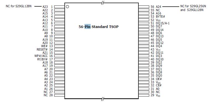 SpecificationsStorage Temperature, Plastic Packages. . . . . . . . .65 to +150
Ambient Temperature with Power Applied . . . . . . 65 to +125
Voltage with Respect to Ground:
VCC (Note 1). . . . . . . . . . . . . . . . . . . . . . . . . . . . . 0.5 V to +4.0 V
VIO . . . . . . . . . . . . . . . . . . . . . . . . . . . . . . . . . . . .0.5 V to +4.0 V
A9, OE#, ACC and RESET# (Note 2) . . . . . . . . . 0.5 V to +12.5 V
All other pins (Note 1) . . . . . . . . . . . . . . . . . . . . 0.5 V to +12.5 V
Output Short Circuit Current (Note 3)200 mA
Notes:
1. Minimum DC voltage on input or I/Os is 0.5 V. During voltage transitions, inputs or I/Os may overshoot VSS to 2.0 V for periods of up to 20 ns. See Figure 7. Maximum DC voltage on input or I/Os is VCC + 0.5 V. During voltage transitions, input or I/O pins may overshoot to VCC + 2.0 V for periods up to 20 ns. See Figure 8.
2. Minimum DC input voltage on pins A9, OE#, ACC, and RESET# is 0.5 V. During voltage transitions, A9, OE#, ACC, and RESET# may overshoot VSS to 2.0 V for periods of up to 20 ns. See Figure 7. Maximum DC input voltage on pin A9, OE#, ACC, and RESET# is +12.5 V which may overshoot to +14.0V for periods up to 20 ns.
3. No more than one output may be shorted to ground at a time. Duration of the short circuit should not be greater than one second.
4. Stresses above those listed under "Absolute Maximum Ratings" may cause permanent damage to the device. This is a stress rating only; functional operation of the device at these or any other conditions above those indicated in the operational sections of this data sheet is not implied. Exposure of the device to absolute maximum rating conditions for extended periods may affect device
reliability.DescriptionThe S29GL256N80TAIV10 devices are 3.0V single power flash memory manufactured using 110 nm MirrorBit technology. The S29GL512N is a 512 Mbit, organized as 33,554,432 words or 67,108,864 bytes. The S29GL256N is a 256 Mbit, organized as 16,777,216 words or 33,554,432 bytes. The S29GL128N is a 128 Mbit, organized as 8,388,608 words or 16,777,216 bytes. The S29GL256N80TAIV10 have a 16-bit wide data bus that can also function as an 8-bit wide data bus by using the BYTE# input. The device can be programmed either in the host system or in standard EPROM programmers.
Access times of S29GL256N80TAIV10 as fast as 80 ns (S29GL128N, S29GL256N) or 90 ns (S29GL512N) are available. Note that each access time has a specific operating voltage range (VCC) and an I/O voltage range (VIO), as specified in the Product Selector Guide and the Ordering Information (512 Mb) sections. The S29GL256N80TAIV10 are offered in a 56- pin TSOP or 64-ball Fortified BGA package. Each device has separate chip enable (CE#), write enable (WE#) and output enable (OE#) controls.
Each device S29GL256N80TAIV10 requires only a single 3.0 volt power supply for both read and write functions. In addition to a VCC input, a high-voltage accelerated program (WP#/ACC) input provides shorter programming times through increased current.
This feature of S29GL256N80TAIV10 is intended to facilitate factory throughput during system production, but may also be used in the field if desired.
The S29GL256N80TAIV10 are entirely command set compatible with the JEDEC singlepower- supply Flash standard. Commands are written to the device using standard microprocessor write timing. Write cycles also internally latch addresses and data needed for the programming and erase operations.
The sector erase architecture of S29GL256N80TAIV10 allows memory sectors to be erased and reprogrammed without affecting the data contents of other sectors. The device is fully erased when shipped from the factory.
Device programming and erasure are initiated through command sequences.
Once a program or erase operation has begun, the host system of S29GL256N80TAIV10 need only poll the DQ7 (Data# Polling) or DQ6 (toggle) status bits or monitor the Ready/Busy# (RY/BY#) output to determine whether the operation is complete. To facilitate programming, an Unlock Bypass mode reduces command sequence overhead by requiring only two write cycles to program data instead of four.
The Enhanced VersatileI/O™ (VIO) control of S29GL256N80TAIV10 allows the host system to set the voltage levels that the device generates and tolerates on all input levels (address, chip control, and DQ input levels) to the same voltage level that is asserted on the VIO pin. This allows the device to operate in a 1.8 V or 3 V system environment as required.
Hardware data protection measures of S29GL256N80TAIV10 include a low VCC detector that automatically inhibits write operations during power transitions. Persistent Sector Protection provides in-system, command-enabled protection of any combination of sectors using a single power supply at VCC. Password Sector Protection prevents unauthorized write and erase operations in any combination of sectors through a user-defined 64-bit password.
The Erase Suspend/Erase Resume feature of S29GL256N80TAIV10 allows the host system to pause an erase operation in a given sector to read or program any other sector and then complete the erase operation. The Program Suspend/Program Resume feature enables the host system to pause a program operation in a given sector to read any other sector and then complete the program operation.

 S29GL256N80TAIV10 Data Sheet