SAA4955TJ

Features: ` 2949264-bit field memory` 245772 *12-bit organization` 3.3 V power supply` Inputs fully TTL compatible when using an extra 5 V power supply` High speed read and write operations` FIFO operations: full word continuous read and write independent read and write pointers (asynchronous read...

product image

SAA4955TJ Picture
SeekIC No. : 004483906 Detail

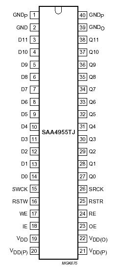
SAA4955TJ: Features: ` 2949264-bit field memory` 245772 *12-bit organization` 3.3 V power supply` Inputs fully TTL compatible when using an extra 5 V power supply` High speed read and write operations` FIFO op...

floor Price/Ceiling Price

Part Number:
SAA4955TJ
Supply Ability:
5000

Price Break

  • Qty
  • 1~5000
  • Unit Price
  • Negotiable
  • Processing time
  • 15 Days
Total Cost: $ 0.00

SeekIC Buyer Protection PLUS - newly updated for 2013!

  • Escrow Protection.
  • Guaranteed refunds.
  • Secure payments.
  • Learn more >>

Month Sales

268 Transactions

Rating

evaluate  (4.8 stars)

Upload time: 2025/12/26

Payment Methods

All payment methods are secure and covered by SeekIC Buyer Protection PLUS.

Notice: When you place an order, your payment is made to SeekIC and not to your seller. SeekIC only pays the seller after confirming you have received your order. We will also never share your payment details with your seller.
Product Details

Description


Features:

` 2949264-bit field memory
` 245772 *12-bit organization
` 3.3 V power supply
` Inputs fully TTL compatible when using an extra 5 V power supply
` High speed read and write operations
` FIFO operations:
full word continuous read and write
independent read and write pointers (asynchronous read and write access)
resettable read and write pointers
` Optional random access by block function (40 words per block) enabled during pointer reset operation
` Quasi static (internal self-refresh and clocking pauses of infinite length)
` Write mask function
` Cascade operation possible
` 16 Mbit CMOS DRAM process technology
` 40-pin SOJ Package.


Pinout

  Connection Diagram


Specifications

SYMBOL PARAMETER CONDITIONS MIN. MAX. UNIT
VDD, VDD(O)

VDD(P)
supply voltages

supply voltage for protection circuits
  -0.5

-0.5
+5

+5.5
V

V
VI input voltage VDD(P) = 5 V
VDD = VDD(O) = VDD(P) = 3.3 V
-0.5
-0.5
+5.5
+3.8
V
V
VO output voltage VDD(P) = 5 V
VDD = VDD(O) = VDD(P) = 3.3 V
-0.5
-0.5
+5
+3.8
V
V
IDD(tot) total supply current   - 200 mA
V voltage difference between GND,
GNDO and GNDP
  -0.5 +0.5 V
IO

Ptot

Tstg

Tj

Tamb
short circuit output current

total power dissipation

storage temperature

junction temperature

ambient temperature
  -

-

-20

0

0
50

750

+150

125

70
mA

mW

°C

°C

°C
Ves electrostatic handling note 1
note 2
-150
-2000
+200
+2000
V
V
Notes
1. Machine model: equivalent to discharging a 200 pF capacitor through a 0 series resistor ('0 ' is actually 0.75 mH + 10 ).
2. Human body model: equivalent to discharging a 100 pF capacitor through a 1500 W series resistor.


Description

The SAA4955TJ is a 2949264-bit field memory designed for advanced TV applications such as 100/120 Hz TV, PALplus, PIP and 3D comb filter. The maximum storage depth is 245772 words ´ 12 bits. A FIFO operation with full word continuous read and write could be used as a data delay, for example. A FIFO operation with asynchronous read and write could be used as a data rate multiplier. Here the data of SAA4955TJ is written once, then read as many times as required without being overwritten by new data.

In addition to the FIFO operations, a random block access mode is accessible during the pointer reset operation. When this mode is enabled, reading and/or writing may begin at, or proceed from, the start address of any of the 6144 blocks. Each block is 40 words in length. Two or more SAA4955TJs can be cascaded to provide greater storage depth or a longer delay, without the need for additional circuitry.

The SAA4955TJ contains separate 12-bit wide serial ports for reading and writing. The ports are controlled and clocked separately, so asynchronous read and write operations are supported. Independent read and write clock rates are possible. Addressing is controlled by read and write address pointers. Before a controlled write operation can begin, the write pointer must be set to zero or to the beginning of a valid address block. Likewise, the read pointer must be set to zero or to the beginning of a valid address block before a controlled read operation can begin.


Customers Who Bought This Item Also Bought

Margin,quality,low-cost products with low minimum orders. Secure your online payments with SeekIC Buyer Protection.
Boxes, Enclosures, Racks
Cables, Wires - Management
Cable Assemblies
Audio Products
Industrial Controls, Meters
RF and RFID
View more