Features: ` Comb filter circuit for luminance and chrominance separation` Applicable for standardsPAL B/G, M and N PAL 4.43 (525 lines, 60 Hz) NTSC M and N NTSC 4.43 (50 and 60 Hz)` Luminance and chrominance bypasses with short delay in case of no filtering` Line-locked system clock; CCIR-compatib...
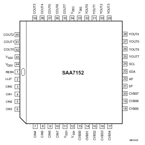
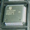
SAA7152: Features: ` Comb filter circuit for luminance and chrominance separation` Applicable for standardsPAL B/G, M and N PAL 4.43 (525 lines, 60 Hz) NTSC M and N NTSC 4.43 (50 and 60 Hz)` Luminance and ch...
SeekIC Buyer Protection PLUS - newly updated for 2013!
268 Transactions
All payment methods are secure and covered by SeekIC Buyer Protection PLUS.

| SYMBOL | PARAMETER | MIN. | MAX. | UNIT |
| VDD | supply voltage (pins 11, 34, 44) | -0.5 | 7.0 | V |
| VI | voltage on all inputs | -0.5 | VDD + 0.5 | V |
| VO | voltage on all outputs (IO max = 20 mA) | -0.5 | VDD + 0.5 | V |
| Ptot | total power dissipation | - | 1.0 | W |
| Tstg | storage temperature range | -65 | 150 | °C |
| Tamb | operating ambient temperature range | 0 | 70 | °C |
| VESD | electrostatic handling(1) for all pins | - | ±2000 | V |
Note
1. Equivalent to discharging a 100 pF capacitor through a 1.5 kW series resistor; inputs and outputs are protected against electrostatic discharge in normal handling. Normal precautions appropriate to handle MOS devices is recommended (see "Handling MOS Devices").
The CMOS digital comb filter circuit SAA7151B is located between video analog-to-digital converters and the video multistandard decoder SAA7151B (not applicable for SAA7191B). The two-dimensional filtering is only appropriate for standard signals from a source with constant phase relationship between subcarrier signal and horizontal frequency. The comb-filter has to be switched off for VTR-signals and for separate VBS and C signals. In VCR and S-Video operation the luminance low-pass and the chrominance bandpass parts can still be used for noise reduction purposes. The processing delay of SAA7151B is:
21× LL27 clocks in active mode, or
3 × LL27 in short delay bypass mode (BYPS = 1)